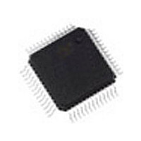
PSD834F2V10MI STMicroelectronics, PSD834F2V10MI Datasheet - Page 83

PSD834F2V10MI
Manufacturer Part Number
PSD834F2V10MI
Description
Manufacturer
STMicroelectronics
Datasheet
1.PSD834F2V10MI.pdf
(95 pages)
Specifications of PSD834F2V10MI
Operating Temperature (max)
85C
Operating Temperature (min)
-40C
Operating Temperature Classification
Industrial
Package Type
PQFP
Mounting
Surface Mount
Pin Count
52
Lead Free Status / RoHS Status
Compliant
- Current page: 83 of 95
- Download datasheet (816Kb)
Figure 43. Peripheral I/O WRITE Timing
Table 51. Port A Peripheral Data Mode WRITE Timing
Note: 1. RD has the same timing as DS, LDS, UDS, and PSEN (in 8031 combined mode).
t
t
t
WLQV–PA
DVQV–PA
WHQZ–PA
Symbol
2. WR has the same timing as the E, LDS, UDS, WRL, and WRH signals.
3. Any input used to select Port A Data Peripheral mode.
4. Data is already stable on Port A.
5. Data stable on ADIO pins to data on Port A.
A / D BUS
ALE /AS
WR to Data Propagation Delay
Data to Port A Data Propagation Delay
WR Invalid to Port A Tri-state
WR
Parameter
ADDRESS
Conditions
tWLQV
(Note
(Note
(Note
2
5
2
(PA)
)
)
)
Min Max Min Max Min Max
tDVQV (PA)
DATA OUT
-10
DATA OUT
PORT A
42
38
33
-15
tWHQZ (PA)
45
40
33
PSD834F2V
-20
AI02898
55
45
35
Unit
83/95
ns
ns
ns
Related parts for PSD834F2V10MI
Image
Part Number
Description
Manufacturer
Datasheet
Request
R

Part Number:
Description:
Flash In-System Programmable (ISP) Peripherals for 8-bit MCUs, 5V
Manufacturer:
STMicroelectronics
Datasheet:

Part Number:
Description:
IC FLASH 2MBIT 90NS 52PLCC
Manufacturer:
STMicroelectronics
Datasheet:

Part Number:
Description:
IC FLASH 2MBIT 70NS 52QFP
Manufacturer:
STMicroelectronics
Datasheet:

Part Number:
Description:
IC FLASH 2MBIT 90NS 52QFP
Manufacturer:
STMicroelectronics
Datasheet:

Part Number:
Description:
IC FLASH 2MBIT 70NS 52PLCC
Manufacturer:
STMicroelectronics
Datasheet:

Part Number:
Description:
IC FLASH 2MBIT 90NS 52PLCC
Manufacturer:
STMicroelectronics
Datasheet:

Part Number:
Description:
IC FLASH 2MBIT 90NS 52QFP
Manufacturer:
STMicroelectronics
Datasheet:

Part Number:
Description:
Manufacturer:
STMicroelectronics
Datasheet:

Part Number:
Description:
Manufacturer:
STMicroelectronics
Datasheet:

Part Number:
Description:
Three Phase Rectifier Bridge
Manufacturer:
POWERSEM [Powersem GmbH]
Datasheet:

Part Number:
Description:
STMicroelectronics [RIPPLE-CARRY BINARY COUNTER/DIVIDERS]
Manufacturer:
STMicroelectronics
Datasheet:

Part Number:
Description:
STMicroelectronics [LIQUID-CRYSTAL DISPLAY DRIVERS]
Manufacturer:
STMicroelectronics
Datasheet:

Part Number:
Description:
BOARD EVAL FOR MEMS SENSORS
Manufacturer:
STMicroelectronics
Datasheet:


