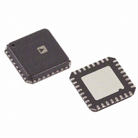
AD9513BCPZ Analog Devices Inc, AD9513BCPZ Datasheet - Page 12

AD9513BCPZ
Manufacturer Part Number
AD9513BCPZ
Description
IC CLOCK DIST 3OUT PLL 32LFCSP
Manufacturer
Analog Devices Inc
Type
Fanout Buffer (Distribution), Dividerr
Datasheet
1.AD9513BCPZ.pdf
(28 pages)
Specifications of AD9513BCPZ
Number Of Circuits
1
Ratio - Input:output
1:3
Differential - Input:output
Yes/Yes
Input
Differential
Output
CMOS, LVDS
Frequency - Max
800MHz
Voltage - Supply
3.135 V ~ 3.465 V
Operating Temperature
-40°C ~ 85°C
Mounting Type
Surface Mount
Package / Case
32-LFCSP
Frequency-max
800MHz
No. Of Multipliers / Dividers
3
No. Of Amplifiers
4
Supply Voltage Range
3.135V To 3.465V
Slew Rate
1V/ns
Operating Temperature Range
-40°C To +85°C
Digital Ic Case Style
LFCSP
Package
32LFCSP EP
Lead Free Status / RoHS Status
Lead free / RoHS Compliant
For Use With
AD9513/PCBZ - BOARD EVAL CLOCK 3CH AD9513
Lead Free Status / RoHS Status
Lead free / RoHS Compliant, Lead free / RoHS Compliant
Available stocks
Company
Part Number
Manufacturer
Quantity
Price
Company:
Part Number:
AD9513BCPZ
Manufacturer:
ADI
Quantity:
3 000
Company:
Part Number:
AD9513BCPZ
Manufacturer:
ADI
Quantity:
140
Company:
Part Number:
AD9513BCPZ-REEL7
Manufacturer:
AD
Quantity:
1 000
Company:
Part Number:
AD9513BCPZ-REEL7
Manufacturer:
ADI
Quantity:
3 000
Part Number:
AD9513BCPZ-REEL7
Manufacturer:
ADI/亚德诺
Quantity:
20 000
AD9513
PIN CONFIGURATION AND FUNCTION DESCRIPTIONS
Note that the exposed paddle on this package is an electrical connection as well as a thermal enhancement. For the device to
function properly, the paddle must be soldered to a PCB land that functions as both a heat dissipation path as well as an electrical
ground.
Table 9. Pin Function Descriptions
Pin No.
1, 4 ,17 ,20, 21,
24, 26, 29, 30
2
3
5
6
7 to16, 25
18
19
22
23
27
28
31
32
SYNCB
CLKB
VREF
CLK
S10
VS
VS
S9
1
2
3
4
5
6
7
8
Figure 5. 32-Lead LFCSP Pin Configuration
Mnemonic
VS
CLK
CLKB
SYNCB
VREF
S10 to S1, S0
OUT2B
OUT2
OUT1B
OUT1
OUT0B
OUT0
GND
RSET
(Not to Scale)
AD9513
TOP VIEW
Description
Power Supply (3.3 V).
Clock Input.
Complementary Clock Input.
Used to Synchronize Outputs.
Provides 2/3 V
Setup Select Pins. These are 4-state logic. The logic levels are V
VREF pin provides 2/3 V
level should be left NC (no connection).
Complementary LVDS/Inverted CMOS Output.
LVDS/CMOS Output.
Complementary LVDS/Inverted CMOS Output. OUT6 includes a delay block.
LVDS/CMOS Output. OUT6 includes a delay block.
Complementary LVDS/Inverted CMOS Output. OUT5 includes a delay block.
LVDS/CMOS Output. OUT5 includes a delay block.
Ground. The exposed paddle on the back of the chip is also GND.
Current Set Resistor to Ground. Nominal value = 4.12 kΩ.
24 VS
23 OUT1
22 OUT1B
21 VS
20 VS
19 OUT2
18 OUT2B
17 VS
S
for use as one of the four logic levels on S0 to S10.
S
. Each pin is internally biased to 1/3 V
Rev. 0 | Page 12 of 28
24
17
16
THERMAL CONNECTION
25
IS AN ELECTRICAL AND
THE EXPOSED PADDLE
Figure 6. Exposed Paddle
S
S
so that a pin requiring that logic
(BOTTOM VIEW)
, GND, 1/3 V
EXPOSED PAD
GND
S
, and 2/3 V
32
9
1
8
S
. The


