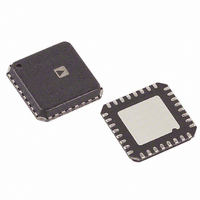
AD9513BCPZ Analog Devices Inc, AD9513BCPZ Datasheet - Page 24

AD9513BCPZ
Manufacturer Part Number
AD9513BCPZ
Description
IC CLOCK DIST 3OUT PLL 32LFCSP
Manufacturer
Analog Devices Inc
Type
Fanout Buffer (Distribution), Dividerr
Datasheet
1.AD9513BCPZ.pdf
(28 pages)
Specifications of AD9513BCPZ
Number Of Circuits
1
Ratio - Input:output
1:3
Differential - Input:output
Yes/Yes
Input
Differential
Output
CMOS, LVDS
Frequency - Max
800MHz
Voltage - Supply
3.135 V ~ 3.465 V
Operating Temperature
-40°C ~ 85°C
Mounting Type
Surface Mount
Package / Case
32-LFCSP
Frequency-max
800MHz
No. Of Multipliers / Dividers
3
No. Of Amplifiers
4
Supply Voltage Range
3.135V To 3.465V
Slew Rate
1V/ns
Operating Temperature Range
-40°C To +85°C
Digital Ic Case Style
LFCSP
Package
32LFCSP EP
Lead Free Status / RoHS Status
Lead free / RoHS Compliant
For Use With
AD9513/PCBZ - BOARD EVAL CLOCK 3CH AD9513
Lead Free Status / RoHS Status
Lead free / RoHS Compliant, Lead free / RoHS Compliant
Available stocks
Company
Part Number
Manufacturer
Quantity
Price
Company:
Part Number:
AD9513BCPZ
Manufacturer:
ADI
Quantity:
3 000
Company:
Part Number:
AD9513BCPZ
Manufacturer:
ADI
Quantity:
140
Company:
Part Number:
AD9513BCPZ-REEL7
Manufacturer:
AD
Quantity:
1 000
Company:
Part Number:
AD9513BCPZ-REEL7
Manufacturer:
ADI
Quantity:
3 000
Part Number:
AD9513BCPZ-REEL7
Manufacturer:
ADI/亚德诺
Quantity:
20 000
AD9513
Termination at the far end of the PCB trace is a second option.
The CMOS outputs of the AD9513 do not supply enough
current to provide a full voltage swing with a low impedance
resistive, far-end termination, as shown in Figure 32. The
far-end termination network should match the PCB trace
impedance and provide the desired switching point. The
reduced signal swing may still meet receiver input requirements
in some applications. This can be useful when driving long
trace lengths on less critical nets.
Because of the limitations of single-ended CMOS clocking,
consider using differential outputs when driving high speed
signals over long traces. The AD9513 offers LVDS outputs that
are better suited for driving long traces where the inherent noise
immunity of differential signaling provides superior
performance for clocking converters.
CMOS
Figure 32. CMOS Output with Far-End Termination
OUT1/OUT1B
SELECTED AS CMOS
10Ω
50Ω
V
S
100Ω
100Ω
3pF
Rev. 0 | Page 24 of 28
SETUP PINS (S0 TO S10)
The setup pins that require a logic level of ⅓ V
bias) should be tied together and bypassed to ground via a
capacitor.
The setup pins that require a logic level of ⅔ V
together, along with the VREF pin, and bypassed to ground via
a capacitor.
POWER AND GROUNDING CONSIDERATIONS AND
POWER SUPPLY REJECTION
Many applications seek high speed and performance under less
than ideal operating conditions. In these application circuits, the
implementation and construction of the PCB is as important
as the circuit design. Proper RF techniques must be used for
device selection, placement, and routing, as well as power
supply bypassing and grounding to ensure optimum
performance.
S
S
(internal self-
should be tied


