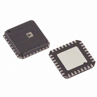
AD9513BCPZ Analog Devices Inc, AD9513BCPZ Datasheet - Page 23

AD9513BCPZ
Manufacturer Part Number
AD9513BCPZ
Description
IC CLOCK DIST 3OUT PLL 32LFCSP
Manufacturer
Analog Devices Inc
Type
Fanout Buffer (Distribution), Dividerr
Datasheet
1.AD9513BCPZ.pdf
(28 pages)
Specifications of AD9513BCPZ
Number Of Circuits
1
Ratio - Input:output
1:3
Differential - Input:output
Yes/Yes
Input
Differential
Output
CMOS, LVDS
Frequency - Max
800MHz
Voltage - Supply
3.135 V ~ 3.465 V
Operating Temperature
-40°C ~ 85°C
Mounting Type
Surface Mount
Package / Case
32-LFCSP
Frequency-max
800MHz
No. Of Multipliers / Dividers
3
No. Of Amplifiers
4
Supply Voltage Range
3.135V To 3.465V
Slew Rate
1V/ns
Operating Temperature Range
-40°C To +85°C
Digital Ic Case Style
LFCSP
Package
32LFCSP EP
Lead Free Status / RoHS Status
Lead free / RoHS Compliant
For Use With
AD9513/PCBZ - BOARD EVAL CLOCK 3CH AD9513
Lead Free Status / RoHS Status
Lead free / RoHS Compliant, Lead free / RoHS Compliant
Available stocks
Company
Part Number
Manufacturer
Quantity
Price
Company:
Part Number:
AD9513BCPZ
Manufacturer:
ADI
Quantity:
3 000
Company:
Part Number:
AD9513BCPZ
Manufacturer:
ADI
Quantity:
140
Company:
Part Number:
AD9513BCPZ-REEL7
Manufacturer:
AD
Quantity:
1 000
Company:
Part Number:
AD9513BCPZ-REEL7
Manufacturer:
ADI
Quantity:
3 000
Part Number:
AD9513BCPZ-REEL7
Manufacturer:
ADI/亚德诺
Quantity:
20 000
APPLICATIONS
USING THE AD9513 OUTPUTS FOR ADC CLOCK
APPLICATIONS
Any high speed, analog-to-digital converter (ADC) is extremely
sensitive to the quality of the sampling clock provided by the
user. An ADC can be thought of as a sampling mixer; any noise,
distortion, or timing jitter on the clock is combined with the
desired signal at the A/D output. Clock integrity requirements
scale with the analog input frequency and resolution, with
higher analog input frequency applications at ≥14-bit resolution
being the most stringent. The theoretical SNR of an ADC is
limited by the ADC resolution and the jitter on the sampling
clock. Considering an ideal ADC of infinite resolution where
the step size and quantization error can be ignored, the available
SNR can be expressed approximately by
where f is the highest analog frequency being digitized.
t
Figure 29 shows the required sampling clock jitter as a function
of the analog frequency and effective number of bits (ENOB).
See Application Note AN-756 and Application Note AN-501 at
www.analog.com.
Many high performance ADCs feature differential clock inputs
to simplify the task of providing the required low jitter clock on
a noisy PCB. (Distributing a single-ended clock on a noisy PCB
can result in coupled noise on the sample clock. Differential
distribution has inherent common-mode rejection that can
provide superior clock performance in a noisy environment.)
The AD9513 features LVDS outputs that provide differential
clock outputs, which enable clock solutions that maximize
converter SNR performance. The input requirements of the
j
is the rms jitter on the sampling clock.
110
100
90
80
70
60
50
40
30
SNR
10
f
A
Figure 29. ENOB and SNR vs. Analog Input Frequency
=
FULL-SCALE SINE WAVE ANALOG FREQUENCY (MHz)
20
×
log
⎡
⎢
⎢
⎣
2π
1
ft
j
⎤
⎥
⎥
⎦
100
SNR = 20log
2πf
1
A
T
J
1k
18
16
14
12
10
8
6
Rev. 0 | Page 23 of 28
ADC (differential or single-ended, logic level, termination)
should be considered when selecting the best clocking/
converter solution.
LVDS CLOCK DISTRIBUTION
The AD9513 provides three clock outputs that are selectable as
either CMOS or LVDS levels. LVDS uses a current mode output
stage. The current is 3.5 mA, which yields 350 mV output swing
across a 100 Ω resistor. The LVDS outputs meet or exceed all
ANSI/TIA/EIA-644 specifications.
A recommended termination circuit for the LVDS outputs
is shown in Figure 30.
See Application Note AN-586 at
information on LVDS.
CMOS CLOCK DISTRIBUTION
The AD9513 provides three outputs that are selectable as either
CMOS or LVDS levels. When selected as CMOS, an output
provides for driving devices requiring CMOS level logic at their
clock inputs.
Whenever single-ended CMOS clocking is used, some of the
following general guidelines should be used.
Point-to-point nets should be designed such that a driver has
one receiver only on the net, if possible. This allows for simple
termination schemes and minimizes ringing due to possible
mismatched impedances on the net. Series termination at the
source is generally required to provide transmission line
matching and/or to reduce current transients at the driver.
The value of the resistor is dependent on the board design and
timing requirements (typically 10 Ω to 100 Ω is used). CMOS
outputs are also limited in terms of the capacitive load or trace
length that they can drive. Typically, trace lengths less than
3 inches are recommended to preserve signal rise/fall times
and preserve signal integrity.
V
LVDS
S
Figure 31. Series Termination of CMOS Output
DIFFERENTIAL (COUPLED)
CMOS
Figure 30. LVDS Output Termination
100Ω
10Ω
MICROSTRIP
www.analog.com
1.0 INCH
60.4Ω
5pF
100Ω
GND
for more
LVDS
V
AD9513
S


