IDT5T915PAGI IDT, Integrated Device Technology Inc, IDT5T915PAGI Datasheet - Page 2
IDT5T915PAGI
Manufacturer Part Number
IDT5T915PAGI
Description
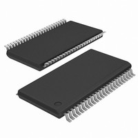
IC CLK BUFFER 1:5 DIFF 48-TSSOP
Manufacturer
IDT, Integrated Device Technology Inc
Type
Fanout Buffer (Distribution)r
Datasheet
1.IDT5T915PAGI8.pdf
(19 pages)
Specifications of IDT5T915PAGI
Number Of Circuits
1
Ratio - Input:output
1:5
Differential - Input:output
Yes/Yes
Input
eHSTL, HSTL, LVPECL, LVTTL
Output
eHSTL, HSTL, LVTTL
Frequency - Max
250MHz
Voltage - Supply
2.4 V ~ 2.6 V
Operating Temperature
-40°C ~ 85°C
Mounting Type
Surface Mount
Package / Case
48-TSSOP
Frequency-max
250MHz
Number Of Outputs
10
Operating Supply Voltage (max)
2.6V
Operating Temp Range
-40C to 85C
Propagation Delay Time
3.5ns
Operating Supply Voltage (min)
2.4V
Mounting
Surface Mount
Pin Count
48
Operating Supply Voltage (typ)
2.5V
Package Type
TSSOP
Quiescent Current
30mA
Operating Temperature Classification
Industrial
Lead Free Status / RoHS Status
Lead free / RoHS Compliant
Other names
5T915PAGI


PIN CONFIGURATION
RECOMMENDED OPERATING RANGE
NOTE:
1. All power supplies should operate in tandem. If V
IDT5T915
2.5V DIFFERENTIAL 1:5 CLOCK BUFFER TERABUFFER
Symbol
V
V
DDQ
V
DD
T
A
T
(1)
(1)
A/V
V
V
V
V
GND
GND
GND
GND
GND
GND
G(+)
V
V
G(-)
DDQ
DDQ
DDQ
DDQ
V
V
RxS
REF
GL
Q
Q
Q
Q
DD
DD
DD
DD
Description
Ambient Operating Temperature
Internal Power Supply Voltage
HSTL Output Power Supply Voltage
Extended HSTL and 1.8V LVTTL Output Power Supply Voltage
2.5V LVTTL Output Power Supply Voltage
Termination Voltage
A
1
1
5
5
1
10
11
12
13
14
15
16
17
18
19
2
3
4
5
6
7
8
9
20
21
22
23
24
TOP VIEW
TSSOP
48
47
46
45
44
43
42
41
40
39
38
37
36
35
34
33
32
31
30
29
28
27
26
25
DD
or V
DDQ
V
V
Q
V
GND
GND
V
GND
GND
GND
V
Q
Q
GND
Q
Q
V
GND
Q
V
GND
GND
V
TxS
DDQ
DDQ
DDQ
DDQ
DDQ
DDQ
DDQ
DDQ
2
2
3
3
4
4
is at maximum, then V
2
DDQ
ABSOLUTE MAXIMUM RATINGS
NOTES:
1. Stresses greater than those listed under ABSOLUTE MAXIMUM RATINGS may cause
2. V
3. Not to exceed 3.6V.
CAPACITANCE
NOTES:
1. This parameter is measured at characterization but not tested.
2. Capacitance applies to all inputs except RxS and TxS.
Symbol
V
V
V
V
V
T
T
Symbol
C
or V
J
DD
DDQ
STG
permanent damage to the device. This is a stress rating only and functional operation
of the device at these or any other conditions above those indicated in the operational
sections of this specification is not implied. Exposure to absolute maximum rating
conditions for extended periods may affect reliability.
need to be met.
I
O
REF
IN
DDQ
DD
and V
(respectively) should be at maximum, and vice-versa.
Power Supply Voltage
Output Power Supply
Input Voltage
Output Voltage
Reference Voltage
Storage Temperature
Junction Temperature
Min.
1.65
–40
2.4
1.4
Input Capacitance
DD
internally operate independently. No power sequencing requirements
Parameter
Description
(3)
V
DDQ
(3)
Typ.
V
+25
(1,2)
2.5
1.5
1.8
DD
(2)
/ 2
(2)
INDUSTRIAL TEMPERATURE RANGE
(T
Min
A
—
= +25°C, F = 1.0MHz)
Max.
1.95
+85
2.6
1.6
Typ.
3.5
–0.5 to V
–0.5 to +3.6
–0.5 to +3.6
–0.5 to +3.6
–0.5 to +3.6
–65 to +165
Max
150
DDQ
Max.
—
+0.5
(1)
Unit
° C
V
V
V
V
V
Unit
Unit
pF
° C
° C
V
V
V
V
V
Related parts for IDT5T915PAGI
Image
Part Number
Description
Manufacturer
Datasheet
Request
R

Part Number:
Description:
TRANSLATION DEVICE DPI 80-PQFP
Manufacturer:
IDT, Integrated Device Technology Inc
Datasheet:
Part Number:
Description:
IDT PART
Manufacturer:
IDT, Integrated Device Technology Inc
Datasheet:
Part Number:
Description:
IC LIU T1/E1/J1 OCTAL 256PBGA
Manufacturer:
IDT, Integrated Device Technology Inc
Datasheet:

Part Number:
Description:
IC FREQ TIMING GENERATOR 28TSSOP
Manufacturer:
IDT, Integrated Device Technology Inc
Datasheet:
Part Number:
Description:
IC CLK DVR PLL 1:10 40VFQFPN
Manufacturer:
IDT, Integrated Device Technology Inc
Datasheet:
Part Number:
Description:
IC CLK FANOUT BUFFER 1:18 32LQFP
Manufacturer:
IDT, Integrated Device Technology Inc
Datasheet:
Part Number:
Description:
IC CLK FANOUT BUFFER 1:18 32LQFP
Manufacturer:
IDT, Integrated Device Technology Inc
Datasheet:
Part Number:
Description:
IC CK505 VREG/RES 56TSSOP
Manufacturer:
IDT, Integrated Device Technology Inc
Datasheet:

Part Number:
Description:
IC SDRAM CLK DVR 1:10 48-TSSOP
Manufacturer:
IDT, Integrated Device Technology Inc
Datasheet:

Part Number:
Description:
IC CLK DVR PLL 1:10 48TSSOP
Manufacturer:
IDT, Integrated Device Technology Inc
Datasheet:
Part Number:
Description:
IC FLEXPC CLK PROGR P4 56-TSSOP
Manufacturer:
IDT, Integrated Device Technology Inc
Datasheet:
Part Number:
Description:
IC FLEXPC CLK PROGR P4 56-TSSOP
Manufacturer:
IDT, Integrated Device Technology Inc
Datasheet:
Part Number:
Description:
IC FLEXPC CLK PROGR P4 56-SSOP
Manufacturer:
IDT, Integrated Device Technology Inc
Datasheet:

Part Number:
Description:
IC PLL CLK DRIVER 2.5V 28-TSSOP
Manufacturer:
IDT, Integrated Device Technology Inc
Datasheet:
Part Number:
Description:
IC CLOCK DRIVER 2.5V 24-TSSOP
Manufacturer:
IDT, Integrated Device Technology Inc
Datasheet: