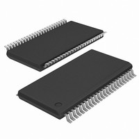
IDT5T915PAGI IDT, Integrated Device Technology Inc, IDT5T915PAGI Datasheet - Page 3

IDT5T915PAGI
Manufacturer Part Number
IDT5T915PAGI
Description
IC CLK BUFFER 1:5 DIFF 48-TSSOP
Manufacturer
IDT, Integrated Device Technology Inc
Type
Fanout Buffer (Distribution)r
Datasheet
1.IDT5T915PAGI8.pdf
(19 pages)
Specifications of IDT5T915PAGI
Number Of Circuits
1
Ratio - Input:output
1:5
Differential - Input:output
Yes/Yes
Input
eHSTL, HSTL, LVPECL, LVTTL
Output
eHSTL, HSTL, LVTTL
Frequency - Max
250MHz
Voltage - Supply
2.4 V ~ 2.6 V
Operating Temperature
-40°C ~ 85°C
Mounting Type
Surface Mount
Package / Case
48-TSSOP
Frequency-max
250MHz
Number Of Outputs
10
Operating Supply Voltage (max)
2.6V
Operating Temp Range
-40C to 85C
Propagation Delay Time
3.5ns
Operating Supply Voltage (min)
2.4V
Mounting
Surface Mount
Pin Count
48
Operating Supply Voltage (typ)
2.5V
Package Type
TSSOP
Quiescent Current
30mA
Operating Temperature Classification
Industrial
Lead Free Status / RoHS Status
Lead free / RoHS Compliant
Other names
5T915PAGI
PIN DESCRIPTION
NOTES:
1. Inputs are capable of translating the following interface standards. User can select between:
2. Outputs are user selectable to drive 2.5V, 1.8V LVTTL, eHSTL, or HSTL interface levels when used with the appropriate V
3. 3-level inputs are static inputs and must be tied to V
4. Because the gate controls are asynchronous, runt pulses are possible. It is the user's responsibility to either time the gate control signals to minimize the possibility of runt
5. Pins listed as LVTTL inputs will accept 2.5V signals when RxS = HIGH or 1.8V signals when RxS = LOW or MID.
Symbol
IDT5T915
2.5V DIFFERENTIAL 1:5 CLOCK BUFFER TERABUFFER
A/V
GND
V
Single-ended 2.5V LVTTL levels
Single-ended 1.8V LVTTL levels
or
Differential 2.5V/1.8V LVTTL levels
Differential HSTL and eHSTL levels
Differential LVEPECL levels
pulses or be able to tolerate them in down stream circuitry.
G(+)
RxS
G(-)
TxS
V
GL
Qn
Qn
DDQ
A
DD
REF
I/O
O
O
I
I
I
I
I
I
I
Adjustable
Adjustable
Adjustable
Adjustable
3 Level
3 Level
LVTTL
LVTTL
LVTTL
Type
PWR
PWR
PWR
(5)
(5)
(5)
(3)
(3)
(1)
(1)
(2)
(2)
Description
Clock input. A is the "true" side of the differential clock input. If operating in single-ended mode, A is the clock input.
Complementary clock input. A/V
mode, A/V
voltage for A:
Gate control for "true", Qn, outputs. When G(+) is LOW, the "true" outputs are enabled. When G(+) is HIGH, the "true" outputs are
asynchronously disabled to the level designated by GL
Gate control for "complementary", Qn, outputs. When G(-) is LOW, the "complementary" outputs are enabled. When G(-) is HIGH,
the "complementary" outputs are asynchronously disabled to the opposite level as GL
Specifies output disable level. If HIGH, "true" outputs disable HIGH and "complementary" outputs disable LOW. If LOW, "true"
outputs disable LOW and "complementary" outputs disable HIGH.
Clock outputs
Complementary clock outputs
Selects single-ended 2.5V LVTTL (HIGH), 1.8V LVTTL (MID) clock input or differential (LOW) clock input
Sets the drive strength of the output drivers to be 2.5V LVTTL (HIGH), 1.8V LVTTL (MID) or HSTL (LOW) compatible. Used in
conjuction with V
Power supply for the device core and inputs
Power supply for the device outputs. When utilizing 2.5V LVTTL outputs, V
Power supply return for all power
REF
DD
is connected to GND. For single-ended operation in differential mode, A/V
2.5V LVTTL
1.8V LVTTL, eHSTL
HSTL
LVEPECL
DDQ
or GND or left floating. These inputs are not hot-insertable or over voltage tolerant.
to set the interface levels.
REF
is the "complementary" side of A if the input is in differential mode. If operating in single-ended
V
V
V
V
REF
REF
REF
REF
3
= 1250mV
= 900mV
= 750mV
= 1082mV
(4)
.
DDQ
should be connected to V
DDQ
(4)
INDUSTRIAL TEMPERATURE RANGE
.
voltage.
REF
should be set to the desired toggle
DD
.


