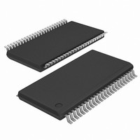
IDT5T915PAGI IDT, Integrated Device Technology Inc, IDT5T915PAGI Datasheet - Page 8

IDT5T915PAGI
Manufacturer Part Number
IDT5T915PAGI
Description
IC CLK BUFFER 1:5 DIFF 48-TSSOP
Manufacturer
IDT, Integrated Device Technology Inc
Type
Fanout Buffer (Distribution)r
Datasheet
1.IDT5T915PAGI8.pdf
(19 pages)
Specifications of IDT5T915PAGI
Number Of Circuits
1
Ratio - Input:output
1:5
Differential - Input:output
Yes/Yes
Input
eHSTL, HSTL, LVPECL, LVTTL
Output
eHSTL, HSTL, LVTTL
Frequency - Max
250MHz
Voltage - Supply
2.4 V ~ 2.6 V
Operating Temperature
-40°C ~ 85°C
Mounting Type
Surface Mount
Package / Case
48-TSSOP
Frequency-max
250MHz
Number Of Outputs
10
Operating Supply Voltage (max)
2.6V
Operating Temp Range
-40C to 85C
Propagation Delay Time
3.5ns
Operating Supply Voltage (min)
2.4V
Mounting
Surface Mount
Pin Count
48
Operating Supply Voltage (typ)
2.5V
Package Type
TSSOP
Quiescent Current
30mA
Operating Temperature Classification
Industrial
Lead Free Status / RoHS Status
Lead free / RoHS Compliant
Other names
5T915PAGI
NOTES:
1. See RECOMMENDED OPERATING RANGE table.
2. For 2.5V LVTTL single-ended operation, the RxS pin is tied HIGH and A/V
3. V
4. V
5. For single-ended operation, in differential mode, A/V
6. Voltage required to maintain a logic HIGH, single-ended operation in differential mode.
7. Voltage required to maintain a logic LOW, single-ended operation in differential mode.
8. Typical values are at V
9. The reference clock input is capable of HSTL, eHSTL, LVEPECL, 1.8V or 2.5V LVTTL operation independent of the device output. The correct input interface table should be
10. For differential mode (RxS = LOW), A and A/V
DC ELECTRICAL CHARACTERISTICS OVER OPERATING RANGE FOR 2.5V
LVTTL
DIFFERENTIAL INPUT AC TEST CONDITIONS FOR LVEPECL
NOTES:
1. The 732mV peak-to-peak input pulse level is specified to allow consistent, repeatable results in an automatic test equipment (ATE) environment. Compliant devices must meet
2. A 1082mV crossing point level is specified to allow consistent, repeatable results in an automatic test equipment (ATE) environment. Compliant devices must meet the V
3. In all cases, input waveform timing is marked at the differential cross-point of the input signals.
4. The input signal edge rate of 1V/ns or greater is to be maintained in the 20% to 80% range of the input waveform.
IDT5T915
2.5V DIFFERENTIAL 1:5 CLOCK BUFFER TERABUFFER
Input Characteristics
Single-Ended Inputs
Differential Inputs
Output Characteristics
Symbol
Symbol
the V
under actual use conditions.
only. The DC differential voltage must be maintained to guarantee retaining the existing HIGH or LOW input. The AC differential voltage must be achieved to guarantee switching
to a new state.
referenced.
V
DIF
CM
V
V
V
V
V
t
V
V
V
V
V
V
V
R
I
I
V
REF
IH
DIF
CM
DIF
THI
IL
OH
OL
, t
IK
IN
IH
IH
IL
IL
X
specifies the minimum input differential voltage (V
specifies the maximum allowable range of (V
DIF
F
(AC) specification under actual use conditions.
(1)
Input HIGH Current
Input LOW Current
Clamp Diode Voltage
DC Input Voltage
DC Input HIGH
DC Input LOW
DC Differential Voltage
DC Common Mode Input Voltage
DC Input HIGH
DC Input LOW
Single-Ended Reference Voltage
Output HIGH Voltage
Output LOW Voltage
Parameter
Input Signal Swing
Differential Input Signal Crossing Point
Input Timing Measurement Reference Level
Input Signal Edge Rate
(2)
DD
Parameter
= 2.5V, V
(5,7,9)
(5,6,9)
(10)
(10)
DDQ
(3,9)
(1)
= V
DD
(4)
, +25°C ambient.
REF
(5,9)
(4,9)
TR
must be at the opposite rail.
REF
+ V
TR
- V
is tied to the DC voltage V
CP
CP
) /2. Differential mode only.
(2)
) required for switching where V
V
V
V
I
I
I
I
OH
OH
OL
OL
DD
DD
DD
(3)
= 12mA
= 100μA
= -12mA
= -100μA
= 2.6V
= 2.6V
= 2.4V, I
Test Conditions
REF
IN
is tied to GND.
= -18mA
REF
8
.
V
V
I
I
= V
= GND/V
TR
is the "true" input level and V
DDQ
/GND
DDQ
V
V
V
REF
DDQ
DDQ
Min.
- 0.3
1150
1.7
0.2
—
—
—
—
—
—
—
—
+ 100
- 0.4
- 0.1
CP
INDUSTRIAL TEMPERATURE RANGE
is the "complement" input level. Differential mode
Crossing Point
Typ.
1250
1250
- 0.7
—
—
Value
1082
732
(8)
1
V
REF
1350
Max
- 1.2
+3.6
0.7
0.4
0.1
±5
±5
—
—
—
—
—
—
- 100
Units
V/ns
X
mV
mV
V
specification
Unit
mV
mV
mV
mV
μA
V
V
V
V
V
V
V
V
V


