IDT5T915PAGI IDT, Integrated Device Technology Inc, IDT5T915PAGI Datasheet
IDT5T915PAGI
Specifications of IDT5T915PAGI


Related parts for IDT5T915PAGI


IDT5T915PAGI Summary of contents
Page 1
IDT5T915 2.5V DIFFERENTIAL 1:5 CLOCK BUFFER TERABUFFER FEATURES: • Guaranteed Low Skew < 25ps (max) • Very low duty cycle distortion < 300ps (max) • High speed propagation delay < 2ns (max) • 250MHz operation • Very low ...
Page 2
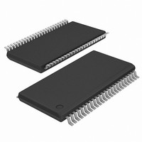
IDT5T915 2.5V DIFFERENTIAL 1:5 CLOCK BUFFER TERABUFFER PIN CONFIGURATION GND 4 45 GND 5 44 G(+) DDQ ...
Page 3
IDT5T915 2.5V DIFFERENTIAL 1:5 CLOCK BUFFER TERABUFFER PIN DESCRIPTION Symbol I/O Type Description ( Adjustable Clock input the "true" side of the differential clock input. If operating in single-ended mode the clock input. A/V ...
Page 4
IDT5T915 2.5V DIFFERENTIAL 1:5 CLOCK BUFFER TERABUFFER INPUT/OUTPUT SELECTION Input 2.5V LVTTL SE 1.8V LVTTL SE 2.5V LVTTL DSE 1.8V LVTTL DSE LVEPECL DSE eHSTL DSE HSTL DSE 2.5V LVTTL DIF 1.8V LVTTL DIF LVEPECL DIF eHSTL DIF HSTL DIF ...
Page 5
IDT5T915 2.5V DIFFERENTIAL 1:5 CLOCK BUFFER TERABUFFER DC ELECTRICAL CHARACTERISTICS OVER OPERATING RANGE FOR HSTL Symbol Parameter Input Characteristics (9) I Input HIGH Current IH (9) I Input LOW Current IL V Clamp Diode Voltage Input Voltage ...
Page 6
IDT5T915 2.5V DIFFERENTIAL 1:5 CLOCK BUFFER TERABUFFER DIFFERENTIAL INPUT AC TEST CONDITIONS FOR HSTL Symbol Parameter (1) V Input Signal Swing DIF V Differential Input Signal Crossing Point X V Input Timing Measurement Reference Level THI Input ...
Page 7
IDT5T915 2.5V DIFFERENTIAL 1:5 CLOCK BUFFER TERABUFFER POWER SUPPLY CHARACTERISTICS FOR eHSTL OUTPUTS Symbol Parameter I Quiescent V Power Supply Current DDQ DD I Quiescent V Power Supply Current DDQQ DDQ I Dynamic V Power Supply DDD DD Current per ...
Page 8
IDT5T915 2.5V DIFFERENTIAL 1:5 CLOCK BUFFER TERABUFFER DIFFERENTIAL INPUT AC TEST CONDITIONS FOR LVEPECL Symbol Parameter V Input Signal Swing (1) DIF V Differential Input Signal Crossing Point X V Input Timing Measurement Reference Level THI ( ...
Page 9
IDT5T915 2.5V DIFFERENTIAL 1:5 CLOCK BUFFER TERABUFFER POWER SUPPLY CHARACTERISTICS FOR 2.5V LVTTL OUTPUTS Symbol Parameter I Quiescent V Power Supply Current DDQ DD I Quiescent V Power Supply Current DDQQ DDQ I Dynamic V Power Supply DDD DD Current ...
Page 10
IDT5T915 2.5V DIFFERENTIAL 1:5 CLOCK BUFFER TERABUFFER DC ELECTRICAL CHARACTERISTICS OVER OPERATING RANGE FOR 1.8V LVTTL (1) Symbol Parameter Input Characteristics (12) I Input HIGH Current IH (12) I Input LOW Current IL V Clamp Diode Voltage ...
Page 11
IDT5T915 2.5V DIFFERENTIAL 1:5 CLOCK BUFFER TERABUFFER POWER SUPPLY CHARACTERISTICS FOR 1.8V LVTTL OUTPUTS Symbol Parameter I Quiescent V Power Supply Current DDQ DD I Quiescent V Power Supply Current DDQQ DDQ I Dynamic V Power Supply DDD DD Current ...
Page 12
IDT5T915 2.5V DIFFERENTIAL 1:5 CLOCK BUFFER TERABUFFER AC ELECTRICAL CHARACTERISTICS OVER OPERATING RANGE Symbol Parameter Skew Parameters Same Device Output Pin-to-Pin Skew Inverting Skew SK INV ( Pulse ...
Page 13
IDT5T915 2.5V DIFFERENTIAL 1:5 CLOCK BUFFER TERABUFFER AC DIFFERENTIAL INPUT SPECIFICATIONS Symbol Parameter t Reference Clock Pulse Width HIGH or LOW (HSTL/eHSTL outputs) W Reference Clock Pulse Width HIGH or LOW (2.5V / 1.8V LVTTL outputs) HSTL/eHSTL/1.8V LVTTL/2.5V LVTTL V ...
Page 14
IDT5T915 2.5V DIFFERENTIAL 1:5 CLOCK BUFFER TERABUFFER DIFFERENTIAL AC TIMING WAVEFORMS 1.8V or 2.5V LVTTL Output Propagation and Skew Waveforms NOTES: 1. For the HSTL and eHSTL outputs, ...
Page 15
IDT5T915 2.5V DIFFERENTIAL 1:5 CLOCK BUFFER TERABUFFER PLH G(+) Qn Qn Differential Gate Disable/Enable Showing Runt Pulse Generation NOTES: 1. The waveforms shown only gate "true" output, Qn shown possible to generate ...
Page 16
IDT5T915 2.5V DIFFERENTIAL 1:5 CLOCK BUFFER TERABUFFER NOTES and t signals are measured from the input passing through V PHL PLH 2. Pulse Skew is calculated using the following expression ...
Page 17
IDT5T915 2.5V DIFFERENTIAL 1:5 CLOCK BUFFER TERABUFFER TEST CIRCUITS AND CONDITIONS Pulse Generator DIFFERENTIAL INPUT TEST CONDITIONS NOTE: 1. This input configuration is used for all input interfaces. For single-ended testing, the V the V 3 inch, ~50Ω ...
Page 18
IDT5T915 2.5V DIFFERENTIAL 1:5 CLOCK BUFFER TERABUFFER V V DDQ DD D.U.T. Qn Test Circuit for SDR Outputs SDR OUTPUT TEST CONDITIONS Symbol V = 2.5V ± 0. Interface Specified DDQ 100 R2 ...
Page 19
IDT5T915 2.5V DIFFERENTIAL 1:5 CLOCK BUFFER TERABUFFER ORDERING INFORMATION XX IDT XXXXX Package Device Type CORPORATE HEADQUARTERS 6024 Silver Creek Valley Road San Jose, CA 95138 X Process I -40°C to +85°C (Industrial) PA Thin Shrink Small Outline Package PAG ...