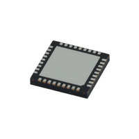
LMX2541SQE3320E/NOPB National Semiconductor, LMX2541SQE3320E/NOPB Datasheet - Page 36

LMX2541SQE3320E/NOPB
Manufacturer Part Number
LMX2541SQE3320E/NOPB
Description
IC PLL FREQ SYNTH W/VCO 36LLP
Manufacturer
National Semiconductor
Series
PowerWise®r
Type
Clock/Frequency Synthesizer (RF)r
Datasheet
1.LMX2541SQE2690ENOPB.pdf
(60 pages)
Specifications of LMX2541SQE3320E/NOPB
Pll
Yes
Input
Clock
Output
Clock
Number Of Circuits
1
Ratio - Input:output
2:2
Differential - Input:output
No/No
Frequency - Max
3.6GHz
Divider/multiplier
Yes/No
Voltage - Supply
3.15 V ~ 3.45 V
Operating Temperature
-40°C ~ 85°C
Mounting Type
Surface Mount
Package / Case
36-LLP
Frequency-max
3.6GHz
Lead Free Status / RoHS Status
Lead free / RoHS Compliant
Other names
LMX2541SQE3320ETR
Available stocks
Company
Part Number
Manufacturer
Quantity
Price
Company:
Part Number:
LMX2541SQE3320E/NOPB
Manufacturer:
NS
Quantity:
673
www.national.com
1.11 LOCK DETECT
The Ftest/LD pin of the LMX2541 can be configured to output
a signal that gives an indication for the PLL being locked.
There are two styles of lock detect; analog and digital. The
analog lock detect signal is more of a legacy feature and con-
sists a series of narrow pulses that correspond to when the
charge pump comes on. These pulses can be integrated with
an external RC filter to create generate a lock detect signal.
Analog lock detect can be configured in a push-pull output or
an open drain output. The analog open drain lock detect sig-
nal can be integrated with a similar RC filter and requires an
additional pull-up resistor. This pull-up resistor can be much
larger than the resistor in the RC filter in order to make un-
balanced time constants for improved sensitivity.
The digital lock detect function can also be selected for the
Ftest/LD pin to give a logic level indication of lock or unlock.
The digital lock detect circuitry works by comparing the dif-
ference between the phase of the inputs to the phase detector
with a RC generated delay of ε. To indicate a locked state
(Lock = HIGH) the phase error must be less than ε for 5 con-
secutive phase detector cycles. Once in lock (Lock = HIGH),
the RC delay is changed to δ. To indicate an out of lock state
(Lock = LOW), the phase error must become greater than δ.
The values of ε and δ are programmable with the DLOCK
word.
Loop Bandwidth
gain in Fastlock
Charge pump
Filter Resistor
Filter Resistor
External Loop
Filter Resistor
Internal Loop
Internal Loop
Parameter
Multiplier
FL_R3_LF
FL_R4_LF
FL_CPG
Symbol
R2pLF
K
Typically choose to be the
sqrt (FL_CPG/CPG)
R2_LF / (K - 1)
largest value.
FL_R3_LF =
FL_R4_LF =
Calculation
R3_LF / K
R4_LF / K
R2pLF =
K =
36
30073306


