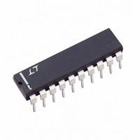
LTC1090CN Linear Technology, LTC1090CN Datasheet - Page 20

LTC1090CN
Manufacturer Part Number
LTC1090CN
Description
IC DATA ACQUIS SYS 10BIT 20-DIP
Manufacturer
Linear Technology
Type
Data Acquisition System (DAS), ADCr
Datasheet
1.LTC1090CNPBF.pdf
(28 pages)
Specifications of LTC1090CN
Resolution (bits)
10 b
Sampling Rate (per Second)
30k
Data Interface
Serial
Voltage Supply Source
Dual ±
Voltage - Supply
5V
Operating Temperature
-40°C ~ 85°C
Mounting Type
Through Hole
Package / Case
20-DIP (0.300", 7.62mm)
Lead Free Status / RoHS Status
Contains lead / RoHS non-compliant
Available stocks
Company
Part Number
Manufacturer
Quantity
Price
Company:
Part Number:
LTC1090CN
Manufacturer:
LT
Quantity:
2 200
Company:
Part Number:
LTC1090CN#PBF
Manufacturer:
Linear Technology
Quantity:
135
APPLICATIO S I FOR ATIO
Input Op Amps
When driving the analog inputs with an op amp it is
important that the op amp settle within the allowed time
(see Figure 10). Again, the “+” and “–” input sampling
times can be extended as described above to accommo-
date slower op amps. Most op amps including the LT1006
and LT1013 single supply op amps can be made to settle
well even with the minimum settling windows of 4µs (“+”
input) and 2µs (“–” input) which occur at the maximum
clock rates (ACLK = 2MHz and SCLK = 1MHz). Figures 11
and 12 show examples of adequate and poor op amp
settling.
RC Input Filtering
It is possible to filter the inputs with an RC network as
shown in Figure 13. For large values of C
capacitive input switching currents are averaged into a net
DC current. Therefore, a filter should be chosen with a
small resistor and large capacitor to prevent DC drops
across the resistor. The magnitude of the DC current is
approximately l
tional to V
33µs, the input current equals 9µA at V
a filter resistor of 50Ω will cause 0.1LSB of full-scale error.
If a larger filter resistor must be used, errors can be
LTC1090
20
Figure 11. Adequate Settling of Op Amp Driving Analog Input
Figure 12. Poor Op Amp Settling can Cause A/D Errors
IN
. When running at the minimum cycle time of
DC
= 60pF x V
U
HORIZONTAL: 20µs/DIV
HORIZONTAL: 1µs/DIV
U
IN
/t
CYC
W
and is roughly propor-
IN
= 5V. In this case,
F
(e.g., 1µF), the
U
eliminated by increasing the cycle time as shown in the
typical curve of Maximum Filter Resistor vs Cycle Time.
Input Leakage Current
Input leakage currents can also create errors if the source
resistance gets too large. For instance, the maximum input
leakage specification of 1µA (at 125°C) flowing through a
source resistance of 1kΩ will cause a voltage drop of 1mV
or 0.2LSB. This error will be much reduced at lower
temperatures because leakage drops rapidly (see typical
curve of Input Channel Leakage Current vs Temperature).
Noise Coupling into Inputs
High source resistance input signals (>500Ω) are more
sensitive to coupling from external sources. It is preferable
to use channels near the center of the package (i.e., CH2 to
CH7) for signals which have the highest output resistance
because they are essentially shielded by the pins on the
package ends (DGND and CH0). Grounding any unused
inputs (especially the end pin, CH0) will also reduce
outside coupling into high source resistances.
4. Sample-and-Hold
Single Ended Inputs
The LTC1090 provides a built-in sample and hold (S&H)
function for all signals acquired in the single ended mode
(COM pin grounded). This sample and hold allows the
LTC1090 to convert rapidly varying signals (see typical
curve of S&H Acquisition Time vs Source Resistance). The
input voltage is sampled during the t
in Figure 10. The sampling interval begins after the fourth
V
IN
R
FILTER
Figure 13. RC Input Filtering
I
DC
C
FILTER
“ + ”
“ – ”
LTC1090
SMPL
LTC1090 • AI18
time as shown
1090fc


