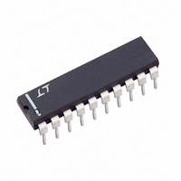
LTC1090CN Linear Technology, LTC1090CN Datasheet - Page 23

LTC1090CN
Manufacturer Part Number
LTC1090CN
Description
IC DATA ACQUIS SYS 10BIT 20-DIP
Manufacturer
Linear Technology
Type
Data Acquisition System (DAS), ADCr
Datasheet
1.LTC1090CNPBF.pdf
(28 pages)
Specifications of LTC1090CN
Resolution (bits)
10 b
Sampling Rate (per Second)
30k
Data Interface
Serial
Voltage Supply Source
Dual ±
Voltage - Supply
5V
Operating Temperature
-40°C ~ 85°C
Mounting Type
Through Hole
Package / Case
20-DIP (0.300", 7.62mm)
Lead Free Status / RoHS Status
Contains lead / RoHS non-compliant
Available stocks
Company
Part Number
Manufacturer
Quantity
Price
Company:
Part Number:
LTC1090CN
Manufacturer:
LT
Quantity:
2 200
Company:
Part Number:
LTC1090CN#PBF
Manufacturer:
Linear Technology
Quantity:
135
V
TYPICAL APPLICATIO
A “Quick Look” Circuit for the LTC1090
Users can get a quick look at the function and timing of the
LTC1090 by using the following simple circuit. REF
D
single ended input, unipolar mode, MSB first format and
16-bit word length. ACLK and SCLK are tied together and
driven by an external clock. CS is driven at 1/64 the clock
rate by the CD4520 and D
pins are tied to a ground plane. The output data from the
D
to trigger on the falling edge of CS.
SNEAK-A-BIT is a trademark of Linear Technology Corp.
IN
IN
OUT
are tied to V
pin can be viewed on an oscilloscope which is set up
CH0
CH1
CH2
CH3
CH4
CH5
CH6
CH7
COM
DGND
LTC1090
4.7µF
A “Quick Look” Circuit for the LTC1090
AGND
REF
REF
ACLK
SCLK
D
V
OUT
D
CS
V
CC
IN
+
–
–
CC
TO OSCILLOSCOPE
selecting a 5V input span, CH7 as a
OTHER CHANNELS
OR SNEAK-A-BIT
f
– 5V TO 5V
OUT
V
CLOCK IN
1MHz MAX
outputs the data. All other
INPUTS
IN
U
CLK
EN
Q1
Q2
Q3
Q4
RESET
f/64
V
SS
9V
LTC1090
CH0
CH1
CH2
CH3
CH4
CH5
CH6
CH7
COM
DGND
RESET
LT1021-5
LTC1090
V
CLK
DD
Q4
Q3
Q2
Q1
EN
AGND
REF
REF
ACLK
SCLK
D
5V
V
OUT
D
CS
V
CC
IN
+
–
–
SNEAK-A-BIT Circuit
+
LTC1090 • TA03
and
0.1
10µF
0.1µF
–5V
SNEAK-A-BIT
The LTC1090’s unique ability to software select the polar-
ity of the differential inputs and the output word length is
used to achieve one more bit of resolution. Using the
circuit below with two conversions and some software, a
2’s complement 10-bit + sign word is returned to memory
inside the MPU. The MC68HC05C4 was chosen as an
example; however, any processor could be used.
Two 10-bit unipolar conversions are performed: the first
over a 0 to 5V span and the second over a 0 to –5V span
(by reversing the polarity of the inputs). The sign of the
input is determined by which of the two spans contained
it. Then the resulting number (ranging from –1023 to 1023
decimal) is converted to 2’s complement notation and
stored in RAM.
CLOCK
2MHz
Scope Trace of LTC1090 “Quick Look” Circuit
Showing A/D Output of 0101010101 (155
DEGLITCHER
D OUT
TIME
CS
TM
SCK
MOSI
MISO
CO
MC68HC05C4
MSB
(B9)
LTC1090 • TA04
(B0)
LSB
FILLS
ZERO
LTC1090
HEX
)
23
1090fc


