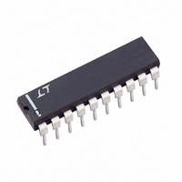
LTC1090CN Linear Technology, LTC1090CN Datasheet - Page 22

LTC1090CN
Manufacturer Part Number
LTC1090CN
Description
IC DATA ACQUIS SYS 10BIT 20-DIP
Manufacturer
Linear Technology
Type
Data Acquisition System (DAS), ADCr
Datasheet
1.LTC1090CNPBF.pdf
(28 pages)
Specifications of LTC1090CN
Resolution (bits)
10 b
Sampling Rate (per Second)
30k
Data Interface
Serial
Voltage Supply Source
Dual ±
Voltage - Supply
5V
Operating Temperature
-40°C ~ 85°C
Mounting Type
Through Hole
Package / Case
20-DIP (0.300", 7.62mm)
Lead Free Status / RoHS Status
Contains lead / RoHS non-compliant
Available stocks
Company
Part Number
Manufacturer
Quantity
Price
Company:
Part Number:
LTC1090CN
Manufacturer:
LT
Quantity:
2 200
Company:
Part Number:
LTC1090CN#PBF
Manufacturer:
Linear Technology
Quantity:
135
APPLICATIO S I FOR ATIO
6. Reduced Reference Operation
The effective resolution of the LTC1090 can be increased
by reducing the input span of the converter. The LTC1090
exhibits good linearity and gain over a wide range of
reference voltages (see typical curves of Linearity and
Gain Error vs Reference Voltage). However, care must be
taken when operating at low values of V
reduced LSB step size and the resulting higher accuracy
requirement placed on the converter. The following factors
must be considered when operating at low V
1. Conversion speed (ACLK frequency)
2. Offset
3. Noise
Conversion Speed with Reduced V
With reduced reference voltages, the LSB step size is
reduced and the LTC1090 internal comparator overdrive is
reduced. With less overdrive, more time is required to
perform a conversion. Therefore, the maximum ACLK
frequency should be reduced when low values of V
used. This is shown in the typical curve of Maximum
Conversion Clock Rate vs Reference Voltage.
Offset with Reduced V
The offset of the LTC1090 has a larger effect on the output
code when the A/D is operated with reduced reference
LTC1090
22
Figure 16. Poor Reference Settling Can Cause A/D Errors
REF
U
HORIZONTAL: 1µs/DIV
U
REF
W
REF
because of the
REF
U
values:
REF
are
voltage. The offset (which is typically a fixed voltage)
becomes a larger fraction of an LSB as the size of the LSB
is reduced. The typical curve of Unadjusted Offset Error vs
Reference Voltage shows how offset in LSBs is related to
reference voltage for a typical value of V
a V
becomes 0.5LSB with a 1V reference and 2.5LSBs with a
0.2V reference. If this offset is unacceptable, it can be
corrected digitally by the receiving system or by offsetting
the “–” input to the LTC1090.
Noise with Reduced V
The total input referred noise of the LTC1090 can be
reduced to approximately 200µV peak-to-peak using a
ground plane, good bypassing, good layout techniques
and minimizing noise on the reference inputs. This noise
is insignificant with a 5V reference but will become a larger
fraction of an LSB as the size of the LSB is reduced. The
typical curve of Noise Error vs Reference Voltage shows
the LSB contribution of this 200µV of noise.
For operation with a 5V reference, the 200µV noise is only
0.04LSB peak-to-peak. In this case, the LTC1090 noise
will contribute virtually no uncertainty to the output code.
However, for reduced references, the noise may become
a significant fraction of an LSB and cause undesirable jitter
in the output code. For example, with a 1V reference, this
same 200µV noise is 0.2LSB peak-to-peak. This will
reduce the range of input voltages over which a stable
output code can be achieved by 0.2LSB. If the reference is
further reduced to 200mV, the 200µV noise becomes
equal to one LSB and a stable code may be difficult to
achieve. In this case averaging readings may be necessary.
This noise data was taken in a very clean setup. Any setup
induced noise (noise or ripple on V
add to the internal noise. The lower the reference voltage
to be used, the more critical it becomes to have a clean,
noise-free setup.
OS
of 0.5mV which is 0.1LSB with a 5V reference
REF
CC
, V
REF
OS
, V
. For example,
IN
or V
–
) will
1090fc


