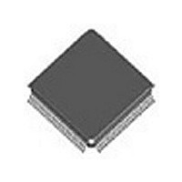
PEB20570FV31XP Lantiq, PEB20570FV31XP Datasheet - Page 33

PEB20570FV31XP
Manufacturer Part Number
PEB20570FV31XP
Description
Manufacturer
Lantiq
Datasheet
1.PEB20570FV31XP.pdf
(308 pages)
Specifications of PEB20570FV31XP
Lead Free Status / Rohs Status
Compliant
- Current page: 33 of 308
- Download datasheet (5Mb)
Table 4
Pin
No.
25
24
23
22
21
18
17
16
38
35
34
33
32
31
30
11
10
12
13
Data Sheet
Symbol In (I)
D7
D6
D5
D4
D3
D2
D1
D0
A6
A5
A4
A3
A2
A1
A0
DREQR O
DREQT O
CS
WR/
R/W
Microprocessor Bus Interface Pins (DELIC-LC)
Out (O)
I/O
The direction of these pins
depends on the value of the
following pins:
CS, RD/DS, WR / R/W and
MODE
I
I
I
During
Reset
I
CLOCK
MASTER
Strap (pull-
down),
refer to
Table 19
ATION
BOOT
Strap (pull-
down),
refer to
Table 19
I
I
EMUL-
After
Reset
I
L
L
I
I
16
Function
Data Bus
When operated in address/data
multiplex mode, this bus is used as a
multiplexed AD bus. The Address pins
are externally connected to the AD bus.
Address Bus (bits 6 ... 0)
When operated in address/data
multiplex mode, this bus is used as a
multiplexed AD bus. The Data pins are
externally connected to the AD bus.
Strap pin
Strap pin
Chip Select
A "low" on this line selects all registers
for read/write operations.
Write (Intel/Infineon Mode)
Indicates a write access.
Read/Write (Motorola Mode)
Indicates the direction of the data
transfer
Pin Description
PEB 20570
PEB 20571
2003-07-31
Related parts for PEB20570FV31XP
Image
Part Number
Description
Manufacturer
Datasheet
Request
R

Part Number:
Description:
Manufacturer:
Lantiq
Datasheet:

Part Number:
Description:
Manufacturer:
Lantiq
Datasheet:

Part Number:
Description:
Manufacturer:
Lantiq
Datasheet:


