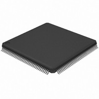
AT94K05AL-25BQU Atmel, AT94K05AL-25BQU Datasheet - Page 107

AT94K05AL-25BQU
Manufacturer Part Number
AT94K05AL-25BQU
Description
IC FPSLIC 5K GATE 25MHZ 144-LQFP
Manufacturer
Atmel
Series
FPSLIC®r
Datasheet
1.AT94K05AL-25AJI.pdf
(204 pages)
Specifications of AT94K05AL-25BQU
Core Type
8-bit AVR
Speed
25MHz
Interface
I²C, UART
Program Sram Bytes
4K-16K
Fpga Sram
2kb
Data Sram Bytes
4K ~ 16K
Fpga Core Cells
256
Fpga Gates
5K
Fpga Registers
436
Voltage - Supply
3 V ~ 3.6 V
Mounting Type
Surface Mount
Operating Temperature
-40°C ~ 85°C
Package / Case
144-LQFP
For Use With
ATSTK594 - BOARD FPSLIC DAUGHTER FOR STK500
Lead Free Status / RoHS Status
Lead free / RoHS Compliant
Eeprom Size
-
Available stocks
Company
Part Number
Manufacturer
Quantity
Price
- Current page: 107 of 204
- Download datasheet (4Mb)
4.26.3
1138I–FPSLI–1/08
Timer/Counter1 in PWM Mode
Timer/Counter1 Input Capture Register – ICR1H AND ICR1L
The input capture register is a 16-bit read-only register.
When the rising or falling edge (according to the input capture edge setting – ICES1) of the sig-
nal at the input capture pin – PE7(ICP) – is detected, the current value of the Timer/Counter1
Register – TCNT1 is transferred to the Input Capture Register – ICR1. In the same cycle, the
input capture flag – ICF1 – is set (one).
Since the Input Capture Register – ICR1 – is a 16-bit register, a temporary register TEMP is
used when ICR1 is read to ensure that both bytes are read simultaneously. When the CPU
reads the low byte ICR1L, the data is sent to the CPU and the data of the high byte ICR1H is
placed in the TEMP register. When the CPU reads the data in the high byte ICR1H, the CPU
receives the data in the TEMP register. Consequently, the low byte ICR1L must be accessed
first for a full 16-bit register read operation.
The TEMP register is also used when accessing TCNT1, OCR1A and OCR1B. If the main pro-
gram and also interrupt routines perform access to registers using TEMP, interrupts must be
disabled during access from the main program and interrupt routine.
When the PWM mode is selected, Timer/Counter1 and the Output Compare Register1A –
OCR1A and the Output Compare Register1B – OCR1B, form a dual 8-, 9- or 10-bit, free-run-
ning, glitch-free and phase correct PWM with outputs on the PE6(OC1A) and PE5(OC1B) pins.
In this mode the Timer/Counter1 acts as an up/down counter, counting up from $0000 to TOP
(see
When the counter value matches the contents of the 8, 9 or 10 least significant bits (depends of
the resolution) of OCR1A or OCR1B, the PD6(OC1A)/PE5(OC1B) pins are set or cleared
according to the settings of the COM1A1/COM1A0 or COM1B1/COM1B0 bits in the
Timer/Counter1 Control Register TCCR1A. Refer to
Alternatively, the Timer/Counter1 can be configured to a PWM that operates at twice the speed
as in the mode described above. Then the Timer/Counter1 and the Output Compare Register1A
– OCR1A and the Output Compare Register1B – OCR1B, form a dual 8-, 9- or 10-bit, free-run-
ning and glitch-free PWM with outputs on the PE6(OC1A) and PE5(OC1B) pins.
As shown in
bits in OCR1A, OCR1B and TCNT1 will automatically be written to zero by the hardware. For
example, bit 9 to 15 will be set to zero in OCR1A, OCR1B and TCNT1 if the 9-bit PWM resolu-
tion is selected. This makes it possible for the user to perform read-modify-write operations in
any of the three resolution modes and the unused bits will be treated as “don’t care”.
Bit
$25 ($45)
$24 ($44)
Read/Write
Initial Value
Table
4-20), where it turns and counts down again to zero before the cycle is repeated.
Table
15
MSB
7
R
R
0
0
4-20, the PWM operates at either 8-, 9- or 10-bit resolution. Note the unused
14
6
R
R
0
0
13
5
R
R
0
0
12
4
R
R
0
0
AT94KAL Series FPSLIC
11
3
R
R
0
0
Table 4-21
10
2
R
R
0
0
for details.
9
1
R
R
0
0
8
LSB
0
R
R
0
0
ICR1H
ICR1L
107
Related parts for AT94K05AL-25BQU
Image
Part Number
Description
Manufacturer
Datasheet
Request
R

Part Number:
Description:
IC FPSLIC 5K GATE 25MHZ 84PLCC
Manufacturer:
Atmel
Datasheet:

Part Number:
Description:
Fpslic Devices Combine 5K Gates of Atmel's Patented AT40K Fpga Architecture, a 20 Mips Avr 8-bit Risc Microprocessor Core, Numerous Fixed Microcontroller Peripheries And up to 36K Bytes of Program And Data SRAM.
Manufacturer:
ATMEL Corporation
Datasheet:

Part Number:
Description:
IC FPSLIC 5K GATE 25MHZ 84PLCC
Manufacturer:
Atmel
Datasheet:

Part Number:
Description:
IC FPSLIC 5K GATE 25MHZ 208PQFP
Manufacturer:
Atmel
Datasheet:

Part Number:
Description:
IC FPSLIC 5K GATE 25MHZ 144LQFP
Manufacturer:
Atmel
Datasheet:

Part Number:
Description:
IC FPSLIC 5K GATE 25MHZ 208PQFP
Manufacturer:
Atmel
Datasheet:

Part Number:
Description:
IC FPSLIC 5K GATE 25MHZ 144LQFP
Manufacturer:
Atmel
Datasheet:

Part Number:
Description:
IC FPSLIC 5K GATE 25MHZ 100-TQFP
Manufacturer:
Atmel
Datasheet:

Part Number:
Description:
Manufacturer:
Atmel
Datasheet:

Part Number:
Description:
Manufacturer:
Atmel
Datasheet:

Part Number:
Description:
Manufacturer:
Atmel
Datasheet:

Part Number:
Description:
5k - 40k Gates Of At40k Fpga With 8-bit Microcontroller, Up To 36k Bytes Of Sram And On-chip Jtag Ice
Manufacturer:
ATMEL Corporation
Datasheet:

Part Number:
Description:
At94k05al 5k - 40k Gates Of At40k Fpga With 8-bit Microcontroller, Up To 36k Bytes Of Sram And On-chip Jtag Ice
Manufacturer:
ATMEL Corporation
Datasheet:

Part Number:
Description:
DEV KIT FOR AVR/AVR32
Manufacturer:
Atmel
Datasheet:


