AT94K05AL-25BQU Atmel, AT94K05AL-25BQU Datasheet - Page 133
AT94K05AL-25BQU
Manufacturer Part Number
AT94K05AL-25BQU
Description
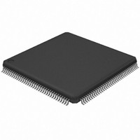
IC FPSLIC 5K GATE 25MHZ 144-LQFP
Manufacturer
Atmel
Series
FPSLIC®r
Datasheet
1.AT94K05AL-25AJI.pdf
(204 pages)
Specifications of AT94K05AL-25BQU
Core Type
8-bit AVR
Speed
25MHz
Interface
I²C, UART
Program Sram Bytes
4K-16K
Fpga Sram
2kb
Data Sram Bytes
4K ~ 16K
Fpga Core Cells
256
Fpga Gates
5K
Fpga Registers
436
Voltage - Supply
3 V ~ 3.6 V
Mounting Type
Surface Mount
Operating Temperature
-40°C ~ 85°C
Package / Case
144-LQFP
For Use With
ATSTK594 - BOARD FPSLIC DAUGHTER FOR STK500
Lead Free Status / RoHS Status
Lead free / RoHS Compliant
Eeprom Size
-
Available stocks
Company
Part Number
Manufacturer
Quantity
Price


4.29.3
4.29.4
1138I–FPSLI–1/08
Multi-processor Communication Mode
UART Control
The Multi-processor Communication Mode enables several Slave MCUs to receive data from a
Master MCU. This is done by first decoding an address byte to find out which MCU has been
addressed. If a particular Slave MCU has been addressed, it will receive the following data bytes
as normal, while the other Slave MCUs will ignore the data bytes until another address byte is
received.
For an MCU to act as a Master MCU, it should enter 9-bit transmission mode (CHR9n in UCS-
RnB set). The 9-bit must be one to indicate that an address byte is being transmitted, and zero
to indicate that a data byte is being transmitted.
For the Slave MCUs, the mechanism appears slightly different for 8-bit and 9-bit Reception
mode. In 8-bit Reception mode (CHR9n in UCSRnB cleared), the stop bit is one for an address
byte and zero for a data byte. In 9-bit Reception mode (CHR9n in UCSRnB set), the 9-bit is one
for an address byte and zero for a data byte, whereas the stop bit is always High.
The following procedure should be used to exchange data in Multi-processor Communication
mode:
UART0 I/O Data Register – UDR0
UART1 I/O Data Register – UDR1
The UDRn register is actually two physically separate registers sharing the same I/O address.
When writing to the register, the UART Transmit Data register is written. When reading from
UDRn, the UART Receive Data register is read.
Bit
$0C ($2C)
Read/Write
Initial Value
Bit
$03 ($23)
Read/Write
Initial Value
1. All Slave MCUs are in Multi-processor Communication Mode (MPCMn in UCSRnA is
2. The Master MCU sends an address byte, and all Slaves receive and read this byte.
3. Each Slave MCU reads the UDRn register and determines if it has been selected. If
4. For each received data byte, the receiving MCU will set the receive complete flag
5. After the last byte has been transferred, the process repeats from step 2.
set).
In the Slave MCUs, the RXCn flag in UCSRnA will be set as normal.
so, it clears the MPCMn bit in UCSRnA, otherwise it waits for the next address byte.
(RXCn in UCSRnA. In 8-bit mode, the receiving MCU will also generate a framing
error (FEn in UCSRnA set), since the stop bit is zero. The other Slave MCUs, which
still have the MPCMn bit set, will ignore the data byte. In this case, the UDRn register
and the RXCn, FEn, or flags will not be affected.
7
MSB
R/W
0
7
MSB
R/W
0
6
R/W
0
6
R/W
0
5
R/W
0
5
R/W
0
4
R/W
0
4
R/W
0
AT94KAL Series FPSLIC
3
R/W
0
3
R/W
0
2
R/W
0
2
R/W
0
1
R/W
0
R/W
1
0
0
LSB
R/W
0
R/W
0
LSB
0
UDR0
UDR1
133
Related parts for AT94K05AL-25BQU
Image
Part Number
Description
Manufacturer
Datasheet
Request
R

Part Number:
Description:
IC FPSLIC 5K GATE 25MHZ 84PLCC
Manufacturer:
Atmel
Datasheet:

Part Number:
Description:
Fpslic Devices Combine 5K Gates of Atmel's Patented AT40K Fpga Architecture, a 20 Mips Avr 8-bit Risc Microprocessor Core, Numerous Fixed Microcontroller Peripheries And up to 36K Bytes of Program And Data SRAM.
Manufacturer:
ATMEL Corporation
Datasheet:
Part Number:
Description:
IC FPSLIC 5K GATE 25MHZ 84PLCC
Manufacturer:
Atmel
Datasheet:

Part Number:
Description:
IC FPSLIC 5K GATE 25MHZ 208PQFP
Manufacturer:
Atmel
Datasheet:

Part Number:
Description:
IC FPSLIC 5K GATE 25MHZ 144LQFP
Manufacturer:
Atmel
Datasheet:
Part Number:
Description:
IC FPSLIC 5K GATE 25MHZ 208PQFP
Manufacturer:
Atmel
Datasheet:
Part Number:
Description:
IC FPSLIC 5K GATE 25MHZ 144LQFP
Manufacturer:
Atmel
Datasheet:

Part Number:
Description:
IC FPSLIC 5K GATE 25MHZ 100-TQFP
Manufacturer:
Atmel
Datasheet:
Part Number:
Description:
Manufacturer:
Atmel
Datasheet:
Part Number:
Description:
Manufacturer:
Atmel
Datasheet:
Part Number:
Description:
Manufacturer:
Atmel
Datasheet:
Part Number:
Description:
5k - 40k Gates Of At40k Fpga With 8-bit Microcontroller, Up To 36k Bytes Of Sram And On-chip Jtag Ice
Manufacturer:
ATMEL Corporation
Datasheet:
Part Number:
Description:
At94k05al 5k - 40k Gates Of At40k Fpga With 8-bit Microcontroller, Up To 36k Bytes Of Sram And On-chip Jtag Ice
Manufacturer:
ATMEL Corporation
Datasheet:

Part Number:
Description:
DEV KIT FOR AVR/AVR32
Manufacturer:
Atmel
Datasheet: