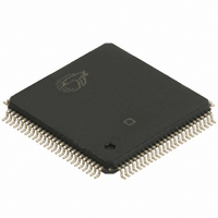
CY7C67300-100AXE Cypress Semiconductor Corp, CY7C67300-100AXE Datasheet - Page 91

CY7C67300-100AXE
Manufacturer Part Number
CY7C67300-100AXE
Description
IC USB HOST/PERIPH CNTRL 100LQFP
Manufacturer
Cypress Semiconductor Corp
Series
EZ-Host™r
Datasheet
1.CY7C67300-100AXI.pdf
(99 pages)
Specifications of CY7C67300-100AXE
Applications
USB Host/Peripheral Controller
Core Processor
CY16
Program Memory Type
ROM (8 kB)
Controller Series
CY7C673xx
Ram Size
16K x 8
Interface
SPI Serial, USB, HPI
Number Of I /o
32
Voltage - Supply
3 V ~ 3.6 V
Operating Temperature
-40°C ~ 125°C
Mounting Type
Surface Mount
Package / Case
100-LQFP
For Use With
CY4640 - KIT MASS STORAGE REF DESIGNCY3663 - KIT DEV EZ-OTG/EZ-HOST
Lead Free Status / RoHS Status
Lead free / RoHS Compliant
IDE Timing
The IDE interface supports PIO mode 0-4 as specified in the Information Technology-AT Attachment–4 with Packet Interface Extension
(ATA/ATAPI-4) Specification, T13/1153D Rev 18.
HSS BYTE Mode Transmit
qt_clk, CPU_A, CPUHSS_cs, CPU_wr are internal signals, included in the diagram to illustrate the relationship between CPU opera-
tions and HSS port operations.
Bit 0 is LSB of data byte. Data bits are HIGH true: HSS_TxD HIGH = data bit value ‘1’.
BT = bit time = 1/baud rate.
HSS Block Mode Transmit
BLOCK mode transmit timing is similar to BYTE mode, except the STOP bit time is controlled by the HSS_GAP value.
The BLOCK mode STOP bit time, t
Transmit Gap register [0xC074].
The default t
BT = bit time = 1/baud rate.
HSS BYTE and BLOCK Mode Receive
Receive data arrives asynchronously relative to the internal clock. Incoming data bit rate may deviate from the programmed baud rate
clock by as much as ±5% (with HSS_RATE value of 23 or higher).
BYTE mode received bytes are buffered in a FIFO. The FIFO not empty condition becomes the RxRdy flag.
BLOCK mode received bytes are written directly to the memory system.
Bit 0 is LSB of data byte. Data bits are HIGH true: HSS_RxD HIGH = data bit value ‘1’.
BT = bit time = 1/baud rate.
Document #: 38-08015 Rev. *J
CPU_A[2:0]
CPUHSS_cs
TxRdy flag
HSS_TxD
CPU_wr
qt_clk
HSS_RxD
HSS_TxD
GAP
is 2 BT.
Byte transmit
triggered by a
CPU write to the
HSS_TxData register
BT +/- 5%
start bit
BT +/- 5%
bit 0
GAP
= (HSS_GAP – 9) BT, where BT is the bit time, and HSS_GAP is the content of the HSS
TxRdy low to start bit delay:
0 min, BT max when starting from IDEL.
bit 1
For back to back transmit, new START Bit
(BT = bit period)
begins immediately following previous STOP bit.
bit 2
start bit
BT
BT
BT
bit 0
bit 3
10 BT +/- 5%
bit 1
t
GAP
bit 4
bit 2
bit 5
bit 3
received byte added to
receive FIFO during the final data bit time
bit 4
start of last data bit to TxRdy high:
0 min, 4 T max.
(T is qt_clk period)
bit 6
bit 5
bit 7
bit 6
stop bit
goes high
bit 7
CPU may start another BYTE
transmit right after TxRdy
CY7C67300
start bit
stop bit
1 or 2 stop bits.
1 stop bit shown.
programmable
Page 91 of 99
start bit
[+] Feedback


