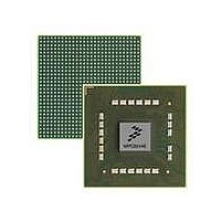
MPC8544VTALF Freescale Semiconductor, MPC8544VTALF Datasheet - Page 109

MPC8544VTALF
Manufacturer Part Number
MPC8544VTALF
Description
MPU POWERQUICC III 783-PBGA
Manufacturer
Freescale Semiconductor
Datasheets
1.MPC8544VTALF.pdf
(117 pages)
2.MPC8544VTALF.pdf
(2 pages)
3.MPC8544VTALF.pdf
(1340 pages)
Specifications of MPC8544VTALF
Processor Type
MPC85xx PowerQUICC III 32-Bit
Speed
667MHz
Voltage
1V
Mounting Type
Surface Mount
Package / Case
783-FCPBGA
Processor Series
MPC85xx
Core
e500
Data Bus Width
32 bit
Maximum Clock Frequency
667 MHz
Maximum Operating Temperature
+ 105 C
Mounting Style
SMD/SMT
Data Ram Size
32 KB
I/o Voltage
1.8 V, 3.3 V
Interface Type
I2C, HSSI, DUART
Minimum Operating Temperature
0 C
Lead Free Status / RoHS Status
Lead free / RoHS Compliant
Features
-
Lead Free Status / Rohs Status
Lead free / RoHS Compliant
Available stocks
Company
Part Number
Manufacturer
Quantity
Price
Company:
Part Number:
MPC8544VTALF
Manufacturer:
Freescale Semiconductor
Quantity:
10 000
Company:
Part Number:
MPC8544VTALFA
Manufacturer:
Freescale Semiconductor
Quantity:
10 000
resistance of the pull-up devices. R
Z
Table 73
nominal OV
21.8
The MPC8544E provides the user with power-on configuration options which can be set through the use
of external pull-up or pull-down resistors of 4.7 kΩ on certain output pins (see customer visible
configuration pins). These pins are generally used as output only pins in normal operation.
While HRESET is asserted however, these pins are treated as inputs. The value presented on these pins
while HRESET is asserted, is latched when HRESET deasserts, at which time the input receiver is disabled
and the I/O circuit takes on its normal function. Most of these sampled configuration pins are equipped
with an on-chip gated resistor of approximately 20 kΩ. This value should permit the 4.7-kΩ resistor to pull
the configuration pin to a valid logic low level. The pull-up resistor is enabled only during HRESET (and
for platform /system clocks after HRESET deassertion to ensure capture of the reset value). When the input
receiver is disabled the pull-up is also, thus allowing functional operation of the pin as an output with
minimal signal quality or delay disruption. The default value for all configuration bits treated this way has
Freescale Semiconductor
Note: Nominal supply voltages. See
0
= (R
Impedance
P
R
R
+ R
summarizes the signal impedance targets. The driver impedances are targeted at minimum V
N
P
Configuration Pin Muxing
DD
N
) ÷ 2.
, 90°C.
MPC8544E PowerQUICC III Integrated Processor Hardware Specifications, Rev. 5
Control, Configuration, Power
Local Bus, Ethernet, DUART,
Management
43 Target
43 Target
Table
Figure 67. Driver Impedance Measurement
Data
Table 73. Impedance Characteristics
P
1.
and R
N
are designed to be close to each other in value. Then,
25 Target
25 Target
PCI
Pad
R
R
OV
OGND
N
P
DD
SW2
SW1
DDR DRAM
20 Target
20 Target
System Design Information
Symbol
Z
Z
0
0
Unit
W
W
DD
109
,


