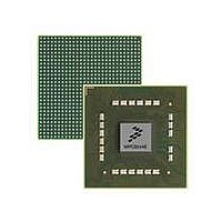
MPC8544VTALF Freescale Semiconductor, MPC8544VTALF Datasheet - Page 58

MPC8544VTALF
Manufacturer Part Number
MPC8544VTALF
Description
MPU POWERQUICC III 783-PBGA
Manufacturer
Freescale Semiconductor
Datasheets
1.MPC8544VTALF.pdf
(117 pages)
2.MPC8544VTALF.pdf
(2 pages)
3.MPC8544VTALF.pdf
(1340 pages)
Specifications of MPC8544VTALF
Processor Type
MPC85xx PowerQUICC III 32-Bit
Speed
667MHz
Voltage
1V
Mounting Type
Surface Mount
Package / Case
783-FCPBGA
Processor Series
MPC85xx
Core
e500
Data Bus Width
32 bit
Maximum Clock Frequency
667 MHz
Maximum Operating Temperature
+ 105 C
Mounting Style
SMD/SMT
Data Ram Size
32 KB
I/o Voltage
1.8 V, 3.3 V
Interface Type
I2C, HSSI, DUART
Minimum Operating Temperature
0 C
Lead Free Status / RoHS Status
Lead free / RoHS Compliant
Features
-
Lead Free Status / Rohs Status
Lead free / RoHS Compliant
Available stocks
Company
Part Number
Manufacturer
Quantity
Price
Company:
Part Number:
MPC8544VTALF
Manufacturer:
Freescale Semiconductor
Quantity:
10 000
Company:
Part Number:
MPC8544VTALFA
Manufacturer:
Freescale Semiconductor
Quantity:
10 000
I
Figure 37
13 I
This section describes the DC and AC electrical characteristics for the I
13.1
Table 51
58
At recommended operating conditions with OV
2
Input high voltage level
Input low voltage level
Low level output voltage
Pulse width of spikes which must be suppressed by the
input filter
Input current each I/O pin (input voltage is between
0.1 × OV
Capacitance for each I/O pin
Notes:
1. Output voltage (open drain or open collector) condition = 3 mA sink current.
2. Refer to the MPC8544EPowerQUICC III Integrated Communications Host Processor Reference Manual for information on
3. I/O pins will obstruct the SDA and SCL lines if OV
C
the digital filter used.
DD
2
provides the DC electrical characteristics for the I
I
C
provides the boundary-scan timing diagram.
External Clock
2
and 0.9 × OV
Data Outputs
Data Outputs
C DC Electrical Characteristics
Data Inputs
Boundary
Boundary
Boundary
MPC8544E PowerQUICC III Integrated Processor Hardware Specifications, Rev. 5
JTAG
Parameter
DD
(max)
t
Output Data Valid
JTKLDX
Figure 37. Boundary-Scan Timing Diagram
Table 51. I
DD
of 3.3 V ± 5%.
t
VM
JTKLDZ
VM = Midpoint Voltage (OV DD /2)
t
JTKLDV
2
C DC Electrical Characteristics
DD
is switched off.
Symbol
t
I2KHKL
V
V
V
C
t
I
OL
JTDVKH
IH
IL
I
I
2
C interfaces.
0.7 × OV
Output Data Valid
–0.3
Data Valid
Min
–10
—
0
0
Input
VM
DD
2
C interfaces of the MPC8544E.
OV
0.3 × OV
0.2 × OV
DD
Max
t
JTDXKH
50
10
10
+ 0.3
DD
DD
Freescale Semiconductor
Unit
μA
pF
ns
V
V
V
Notes
—
—
—
1
2
3


