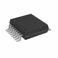
AD5933YRSZ Analog Devices Inc, AD5933YRSZ Datasheet - Page 21

AD5933YRSZ
Manufacturer Part Number
AD5933YRSZ
Description
IC NTWK ANALYZER 12B 1MSP 16SSOP
Manufacturer
Analog Devices Inc
Datasheet
1.AD5933YRSZ.pdf
(44 pages)
Specifications of AD5933YRSZ
Resolution (bits)
12 b
Master Fclk
16.776MHz
Voltage - Supply
2.7 V ~ 5.5 V
Operating Temperature
-40°C ~ 125°C
Mounting Type
Surface Mount
Package / Case
16-SSOP
Supply Voltage Range
2.7V To 5.5V
Operating Temperature Range
-40°C To +125°C
Digital Ic Case Style
SSOP
No. Of Pins
16
Frequency Max
0.1MHz
Termination Type
SMD
Pin Count
16
Screening Level
Automotive
Package Type
SSOP
Filter Terminals
SMD
Rohs Compliant
Yes
Communication Function
Network Analyzer
Lead Free Status / RoHS Status
Lead free / RoHS Compliant
For Use With
EVAL-AD5933EBZ - BOARD EVALUATION FOR AD5933
Tuning Word Width (bits)
-
Lead Free Status / Rohs Status
Compliant
Other names
AD5933BRSZ
Q2204656A
Q2204656A
Available stocks
Company
Part Number
Manufacturer
Quantity
Price
Company:
Part Number:
AD5933YRSZ
Manufacturer:
ADI
Quantity:
5 000
Company:
Part Number:
AD5933YRSZ
Manufacturer:
Fujitsu
Quantity:
500
Part Number:
AD5933YRSZ
Manufacturer:
ADI/亚德诺
Quantity:
20 000
MEASURING THE PHASE ACROSS AN IMPEDANCE
The AD5933 returns a complex output code made up of sepa-
rate real and imaginary components. The real component is
stored at Register Address 0x94 and Register Address 0x95 and
the imaginary component is stored at Register Address 0x96
and Register Address 0x97 after each sweep measurement.
These correspond to the real and imaginary components of
the DFT and not the resistive and reactive components of the
impedance under test.
For example, it is a very common misconception to assume
that if a user is analyzing a series RC circuit, the real value
stored in Register Address 0x94 and Register Address 0x95
and the imaginary value stored at Register Address 0x96
and Register Address 0x97 correspond to the resistance and
capacitive reactance, respectfully. However, this is incorrect
because the magnitude of the impedance (|Z|) can be calculated
by calculating the magnitude of the real and imaginary compo-
nents of the DFT given by the following formula:
After each measurement, multiply it by the calibration term and
invert the product. The magnitude of the impedance is, therefore,
given by the following formula:
Where gain factor is given by
The user must calibrate the AD5933 system for a known
impedance range to determine the gain factor before any valid
measurement can take place. Therefore, the user must know the
impedance limits of the complex impedance (Z
sweep frequency range of interest. The gain factor is determined
by placing a known impedance between the input/output of the
AD5933 and measuring the resulting magnitude of the code.
The AD5933 system gain settings need to be chosen to place
the excitation signal in the linear region of the on-board ADC.
Because the AD5933 returns a complex output code made up of
real and imaginary components, the user can also calculate the
phase of the response signal through the AD5933 signal path.
The phase is given by the following formula:
The phase measured by Equation 3 accounts for the phase shift
introduced to the DDS output signal as it passes through the
internal amplifiers on the transmit and receive side of the
AD5933 along with the low-pass filter and also the impedance
connected between the VOUT and VIN pins of the AD5933.
Phase(rads) = tan
Gain
Impedance
Magnitude
Factor
=
=
=
Gain
⎛
⎜
⎝
R
Admittance
2
−1
+
(I/R)
Code
Factor
I
2
1
×
⎞
⎟
⎠
Magnitude
=
⎛
⎜ ⎜
⎝
Impedance
Magnitude
1
UNKNOWN
⎞
⎟ ⎟
⎠
) for the
Rev. C | Page 21 of 44
(3)
The parameters of interest for many users are the magnitude of
the impedance (|Z
The measurement of the impedance phase (ZØ) is a two step
process.
The first step involves calculating the AD5933 system phase.
The AD5933 system phase can be calculated by placing a
resistor across the VOUT and VIN pins of the AD5933 and
calculating the phase (using Equation 3) after each measure-
ment point in the sweep. By placing a resistor across the
VOUT and VIN pins, there is no additional phase lead or lag
introduced to the AD5933 signal path and the resulting phase
is due entirely to the internal poles of the AD5933, that is, the
system phase.
Once the system phase has been calibrated using a resistor, the
second step involves calculating the phase of any unknown
impedance by inserting the unknown impedance between the
VIN and VOUT terminals of the AD5933 and recalculating the
new phase (including the phase due to the impedance) using
the same formula. The phase of the unknown impedance (ZØ)
is given by the following formula:
where:
connected between VIN and VOUT.
Φunknown is the phase of the system with the unknown
impedance connected between VIN and VOUT.
ZØ is the phase due to the impedance, that is, the impedance
phase.
Note that it is possible to calculate the gain factor and to
calibrate the system phase using the same real and imaginary
component values when a resistor is connected between the
VOUT and VIN pins of the AD5933, for example, measuring
the impedance phase (ZØ) of a capacitor.
The excitation signal current leads the excitation signal voltage
across a capacitor by −90 degrees. Therefore, an approximate
−90 degree phase difference exists between the system phase
responses measured with a resistor and that of the system phase
responses measured with a capacitive impedance.
As previously outlined, if the user would like to determine the
phase angle of capacitive impedance (ZØ), the user first has to
determine the system phase response (
this from the phase calculated with the capacitor connected
between VOUT and VIN (Φunknown).
∇
system
Z
Ø
=
is the phase of the system with a calibration resistor
(
Φ
unknown
UNKNOWN
−
∇
|) and the impedance phase (ZØ).
system
)
∇
system
) and subtract
AD5933


