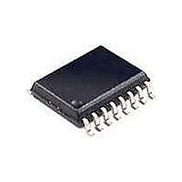
SI3050-KT Silicon Laboratories Inc, SI3050-KT Datasheet - Page 37

SI3050-KT
Manufacturer Part Number
SI3050-KT
Description
IC VOICE DAA GCI/PCM/SPI 20TSSOP
Manufacturer
Silicon Laboratories Inc
Type
Chipsetr
Specifications of SI3050-KT
Package / Case
20-TSSOP
Function
Data Access Arrangement (DAA)
Interface
PCM, Serial, SPI
Number Of Circuits
1
Voltage - Supply
3 V ~ 3.6 V
Current - Supply
8.5mA
Operating Temperature
0°C ~ 70°C
Mounting Type
Surface Mount
Includes
Line Voltage Monitor, Loop Current Monitor, Overload Detection, Parallel Handset Detection, Polarity Reversal Detection, TIP and
Product
Modem Chip
Supply Voltage (min)
3 V
Supply Current
8.5 mA
Maximum Operating Temperature
+ 70 C
Minimum Operating Temperature
0 C
Mounting Style
SMD/SMT
Lead Free Status / RoHS Status
Contains lead / RoHS non-compliant
Power (watts)
-
Lead Free Status / RoHS Status
Lead free / RoHS Compliant, Contains lead / RoHS non-compliant
Available stocks
Company
Part Number
Manufacturer
Quantity
Price
Part Number:
SI3050-KT
Manufacturer:
SILICONIX
Quantity:
20 000
Company:
Part Number:
SI3050-KTR
Manufacturer:
NEC
Quantity:
947
Part Number:
SI3050-KTR
Manufacturer:
SILICON LABS/芯科
Quantity:
20 000
Note: This table denotes pin functionality after the rising edge
SDI_THRU
Table 20. PCM or GCI Highway Mode Selection
Pin Name
Note: Values shown are the states of the pins at the rising
FSYNC
SCLK
PCLK
SDO
DTX
DRX
Table 21. Pin Functionality in PCM or GCI
SDI
CS
SCLK
of RESET and mode selection.
edge of RESET.
1
0
0
SPI Serial Data Output
pin for Daisy Chaining
subsequent device in
SPI Data Throughput
SPI Serial Data Input
Operation (Connects
to the SDI pin of the
PCM Data Transmit
PCM Data Receive
PCM Frame Sync
PCM Input Clock
the daisy chain)
SPI Chip Select
SPI Clock Input
PCM Mode
SDI
Highway Mode
X
0
1
Input
B2 Channel used
B1 Channel used
Mode Selected
PCM Mode
GCI Mode,
GCI Mode,
GCI Data Transmit
GCI Data Receive
GCI Frame Sync
PCM/GCI Mode
GCI Input Clock
B1/B2 Channel
Selector, bit 2
Selector, bit 1
Selector, bit 0
GCI Mode
Sub-frame
Sub-frame
Sub-frame
Selector
Selector
Input
Rev. 1.0
PCM Highway
The Si3050 contains a flexible programmable interface
for the transmission and reception of digital PCM
samples. PCM data transfer is controlled via the PCLK
and FSYNC inputs, the PCM Transmit and Receive
Start Count registers (Registers 34–37), and the PCM
Mode Select register (Register 33). The interface can
be configured to support from 4 to 128 8-bit timeslots in
each frame, which corresponds to PCLK frequencies of
256 kHz to 8.192 MHz in power of 2 increments. Time
slot assignment and data delay from FSYNC edge are
handled via the TXS and RXS registers. These 10-bit
values are programmed with the number of PCLK
cycles following the rising edge of FSYNC until the data
transfer begins. Because the Si3050 looks for the rising
edge of FSYNC, both long and short FSYNC pulse
widths can be accommodated. A value of 0 in the PCM
Transmit and Receive Start Count registers signifies
that the MSB of the data should occur in the same cycle
as the rising edge of FSYNC. By setting the correct
starting point of the data, the Si3050 can operate with
buses having multiple devices requiring different time
slots. The DTX pin is high impedance except during
transmission of an 8-bit PCM sample. DTX returns to
high impedance either on the negative edge of PCLK
during the LSB or on the positive edge of PCLK
following the LSB. This behavior is based on the setting
of the TRI bit in the PCM Mode Select register.
Tristating on the negative edge allows the transmission
of data by multiple sources in adjacent timeslots without
the risk of driver contention. In addition to 8-bit data
modes, a 16-bit linear mode is also provided. This mode
can be activated via the PCMF bits in the PCM Mode
Select register. Double-clocked timing also is supported
in which the duration of a data bit is two PCLK cycles.
This mode is activated via the PHCF bit in the PCM
Mode Select register. Setting the TXS or RXS registers
greater than the number of PCLK cycles in a sample
period stops data transmission or reception. Figures
28–31 illustrate the usage of the PCM highway interface
to adapt to common PCM standards.
Si3050
37


