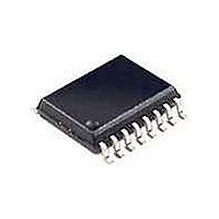
SI3050-KT Silicon Laboratories Inc, SI3050-KT Datasheet - Page 83

SI3050-KT
Manufacturer Part Number
SI3050-KT
Description
IC VOICE DAA GCI/PCM/SPI 20TSSOP
Manufacturer
Silicon Laboratories Inc
Type
Chipsetr
Specifications of SI3050-KT
Package / Case
20-TSSOP
Function
Data Access Arrangement (DAA)
Interface
PCM, Serial, SPI
Number Of Circuits
1
Voltage - Supply
3 V ~ 3.6 V
Current - Supply
8.5mA
Operating Temperature
0°C ~ 70°C
Mounting Type
Surface Mount
Includes
Line Voltage Monitor, Loop Current Monitor, Overload Detection, Parallel Handset Detection, Polarity Reversal Detection, TIP and
Product
Modem Chip
Supply Voltage (min)
3 V
Supply Current
8.5 mA
Maximum Operating Temperature
+ 70 C
Minimum Operating Temperature
0 C
Mounting Style
SMD/SMT
Lead Free Status / RoHS Status
Contains lead / RoHS non-compliant
Power (watts)
-
Lead Free Status / RoHS Status
Lead free / RoHS Compliant, Contains lead / RoHS non-compliant
Available stocks
Company
Part Number
Manufacturer
Quantity
Price
Part Number:
SI3050-KT
Manufacturer:
SILICONIX
Quantity:
20 000
Company:
Part Number:
SI3050-KTR
Manufacturer:
NEC
Quantity:
947
Part Number:
SI3050-KTR
Manufacturer:
SILICON LABS/芯科
Quantity:
20 000
Register 33. PCM/SPI Mode Select
Reset settings = 0000_0000
Name PCML SPIM PCME
Type
Bit
4:3
Bit
7
6
5
2
1
0
PCMF[1:0]
Reserved
R/W
D7
PCME
PCML
Name
PHCF
SPIM
TRI
R/W
D6
PCM Analog Loopback.
0 = Normal operation.
1 = Enables analog data to be received from the line, converted to digital data and trans-
mitted across the ISOcap link. The data passes through the RX filter and is looped back
through the TX filter and is transmitted back out to the line.
SPI Mode.
0 = Normal Operation; SDO tri-states on rising edge of CS.
1 = Causes SDO to tri-state on rising edge of LSB of SCLK.
PCM Enable (Registers 34–37 should be set before PCM transfers are enabled).
0 = Disable PCM transfers.
1 = Enable PCM transfers.
PCM Data Format.
00 = A-Law. Signed magnitude data format (refer to Table 23 on page 42).
01 = µ -Law. Signed magnitude data format (refer to Table 22 on page 41).
10 = 8-bit linear. The top 8-bits of the 16-bit linear signal are transferred, and the bottom
8-bits are discarded (2s complement data format).
11 = 16-bit linear (2s complement data format).
PCM Highway Clock Format.
0 = 1 PCLK per data bit.
1 = 2 PCLKs per data bit.
Tri-state Bit 0.
0 = Tri-state bit 0 on positive edge of PCLK.
1 = Tri-state bit 0 on negative edge of PCLK.
Always write this bit to zero.
R/W
D5
D4
PCMF[1:0]
R/W
D3
R/W
D2
0
Rev. 1.0
PHCF
R/W
D1
Function
R/W
TRI
D0
Si3050
83


