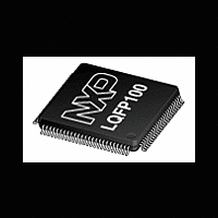
LPC2921_23_25 NXP Semiconductors, LPC2921_23_25 Datasheet - Page 2

LPC2921_23_25
Manufacturer Part Number
LPC2921_23_25
Description
The LPC2921/2923/2925 combine an ARM968E-S CPU core with two integrated TCMblocks operating at frequencies of up to 125 MHz, Full-speed USB 2
Manufacturer
NXP Semiconductors
Datasheet
1.LPC2921_23_25.pdf
(84 pages)
- Current page: 2 of 84
- Download datasheet (552Kb)
NXP Semiconductors
LPC2921_23_25_3
Product data sheet
Other peripherals:
Up to 60 general-purpose I/O pins with programmable pull-up, pull-down, or bus
keeper.
Vectored Interrupt Controller (VIC) with 16 priority levels.
Up to 16 level-sensitive external interrupt pins, including USB, CAN and LIN wake-up
features.
Configurable clock out pin for driving external system clocks.
Processor wake-up from power-down via external interrupt pins and CAN or LIN
activity.
Flexible Reset Generator Unit (RGU) able to control resets of individual modules.
Flexible Clock-Generation Unit (CGU) able to control clock frequency of individual
modules:
Second, dedicated CGU with its own PLL generates the USB clock and a configurable
clock output.
Highly configurable system Power Management Unit (PMU):
Standard ARM test and debug interface with real-time in-circuit emulator.
Boundary-scan test supported.
ETM/ETB debug functions with 8 kB of dedicated SRAM also accessible for
application code and data storage.
Dual power supply:
100-pin LQFP package.
−40 °C to +85 °C ambient operating temperature range.
Two 10-bit ADCs, 8-channels each, with 3.3 V measurement range provide 8
analog inputs each with conversion times as low as 2.44 μs per channel. Each
channel provides a compare function to minimize interrupts.
Multiple trigger-start option for all ADCs: timer, PWM, other ADC and external
signal input.
Four 32-bit timers each containing four capture-and-compare registers linked to
I/Os.
Four six-channel PWMs (Pulse Width Modulators) with capture and trap
functionality.
Two dedicated 32-bit timers to schedule and synchronize PWM and ADC.
Quadrature encoder interface that can monitor one external quadrature encoder.
32-bit watchdog with timer change protection, running on safe clock.
On-chip very low-power ring oscillator; fixed frequency of 0.4 MHz; always on to
provide a Safe_Clock source for system monitoring.
On-chip crystal oscillator with a recommended operating range from 10 MHz to
25 MHz. PLL input range 10 MHz to 25 MHz.
On-chip PLL allows CPU operation up to a maximum CPU rate of 125 MHz.
Generation of up to 11 base clocks.
Seven fractional dividers.
clock control of individual modules.
allows minimization of system operating power consumption in any configuration.
CPU operating voltage: 1.8 V ± 5 %.
I/O operating voltage: 2.7 V to 3.6 V; inputs tolerant up to 5.5 V.
All information provided in this document is subject to legal disclaimers.
Rev. 03 — 14 April 2010
ARM9 microcontroller with CAN, LIN, and USB
LPC2921/2923/2925
© NXP B.V. 2010. All rights reserved.
2 of 84
Related parts for LPC2921_23_25
Image
Part Number
Description
Manufacturer
Datasheet
Request
R
Part Number:
Description:
Arm9 Microcontroller With Can, Lin, And Usb Device
Manufacturer:
NXP Semiconductors
Datasheet:
Part Number:
Description:
(LPC2921 - LPC2925) ARM9 microcontroller
Manufacturer:
NXP Semiconductors
Datasheet:
Part Number:
Description:
NXP Semiconductors designed the LPC2420/2460 microcontroller around a 16-bit/32-bitARM7TDMI-S CPU core with real-time debug interfaces that include both JTAG andembedded trace
Manufacturer:
NXP Semiconductors
Datasheet:

Part Number:
Description:
NXP Semiconductors designed the LPC2458 microcontroller around a 16-bit/32-bitARM7TDMI-S CPU core with real-time debug interfaces that include both JTAG andembedded trace
Manufacturer:
NXP Semiconductors
Datasheet:
Part Number:
Description:
NXP Semiconductors designed the LPC2468 microcontroller around a 16-bit/32-bitARM7TDMI-S CPU core with real-time debug interfaces that include both JTAG andembedded trace
Manufacturer:
NXP Semiconductors
Datasheet:
Part Number:
Description:
NXP Semiconductors designed the LPC2470 microcontroller, powered by theARM7TDMI-S core, to be a highly integrated microcontroller for a wide range ofapplications that require advanced communications and high quality graphic displays
Manufacturer:
NXP Semiconductors
Datasheet:
Part Number:
Description:
NXP Semiconductors designed the LPC2478 microcontroller, powered by theARM7TDMI-S core, to be a highly integrated microcontroller for a wide range ofapplications that require advanced communications and high quality graphic displays
Manufacturer:
NXP Semiconductors
Datasheet:
Part Number:
Description:
The Philips Semiconductors XA (eXtended Architecture) family of 16-bit single-chip microcontrollers is powerful enough to easily handle the requirements of high performance embedded applications, yet inexpensive enough to compete in the market for hi
Manufacturer:
NXP Semiconductors
Datasheet:
Part Number:
Description:
The XA-S3 device is a member of Philips Semiconductors? XA(eXtended Architecture) family of high performance 16-bitsingle-chip microcontrollers
Manufacturer:
NXP Semiconductors
Datasheet:

Part Number:
Description:
The NXP BlueStreak LH75401/LH75411 family consists of two low-cost 16/32-bit System-on-Chip (SoC) devices
Manufacturer:
NXP Semiconductors
Datasheet:

Part Number:
Description:
The NXP LPC3130/3131 combine an 180 MHz ARM926EJ-S CPU core, high-speed USB2
Manufacturer:
NXP Semiconductors
Datasheet:

Part Number:
Description:
The NXP LPC3141 combine a 270 MHz ARM926EJ-S CPU core, High-speed USB 2
Manufacturer:
NXP Semiconductors

Part Number:
Description:
The NXP LPC3143 combine a 270 MHz ARM926EJ-S CPU core, High-speed USB 2
Manufacturer:
NXP Semiconductors

Part Number:
Description:
The NXP LPC3152 combines an 180 MHz ARM926EJ-S CPU core, High-speed USB 2
Manufacturer:
NXP Semiconductors


