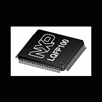
LPC2921_23_25 NXP Semiconductors, LPC2921_23_25 Datasheet - Page 4

LPC2921_23_25
Manufacturer Part Number
LPC2921_23_25
Description
The LPC2921/2923/2925 combine an ARM968E-S CPU core with two integrated TCMblocks operating at frequencies of up to 125 MHz, Full-speed USB 2
Manufacturer
NXP Semiconductors
Datasheet
1.LPC2921_23_25.pdf
(84 pages)
- Current page: 4 of 84
- Download datasheet (552Kb)
NXP Semiconductors
4. Block diagram
LPC2921_23_25_3
Product data sheet
Fig 1.
TIMER0/1 MTMR
LPC2921/2923/2925
ACCEPTANCE
QUADRATURE
MANAGEMENT
UART/LIN0/1
3.3 V ADC1/2
PWM0/1/2/3
Grey-shaded blocks represent peripherals and memory regions accessible by the GPDMA.
LPC2921/2923/2925 block diagram
GENERATION
GENERATION
ENCODER
GLOBAL
FILTER
POWER
CAN0/1
I
CLOCK
RESET
2
UNIT
UNIT
UNIT
C0/1
CONTROLLER
INTERRUPT
VECTORED
networking subsystem
power, clock, and
reset subsystem
MSC subsystem
AHB TO DTL
AHB TO DTL
AHB TO APB
AHB TO APB
BRIDGE
BRIDGE
BRIDGE
BRIDGE
All information provided in this document is subject to legal disclaimers.
1 master
2 slaves
ITCM
16 kB
slave
slave
slave
slave
Rev. 03 — 14 April 2010
TEST/DEBUG
ARM968E-S
INTERFACE
8 kB SRAM
interface
JTAG
MATRIX
MULTI-
LAYER
AHB
master
master
master
slave
slave
slave
slave
slave
slave
slave
DTCM
16 kB
ARM9 microcontroller with CAN, LIN, and USB
peripheral subsystem
general subsystem
EMBEDDED SRAM 16 kB
EMBEDDED SRAM 16 kB
AHB TO APB
AHB TO APB
GPDMA CONTROLLER
GPDMA REGISTERS
EMBEDDED FLASH
BRIDGE
BRIDGE
(LPC2925 only)
512/256/128 kB
CONTROLLER
USB DEVICE
LPC2921/2923/2925
GENERAL PURPOSE I/O
SYSTEM CONTROL
CHIP FEATURE ID
EVENT ROUTER
EEPROM
16 kB
RS-485 UART0/1
TIMER 0/1/2/3
PORTS 0/1/5
SPI0/1/2
© NXP B.V. 2010. All rights reserved.
WDT
002aae224
4 of 84
Related parts for LPC2921_23_25
Image
Part Number
Description
Manufacturer
Datasheet
Request
R
Part Number:
Description:
Arm9 Microcontroller With Can, Lin, And Usb Device
Manufacturer:
NXP Semiconductors
Datasheet:
Part Number:
Description:
(LPC2921 - LPC2925) ARM9 microcontroller
Manufacturer:
NXP Semiconductors
Datasheet:
Part Number:
Description:
NXP Semiconductors designed the LPC2420/2460 microcontroller around a 16-bit/32-bitARM7TDMI-S CPU core with real-time debug interfaces that include both JTAG andembedded trace
Manufacturer:
NXP Semiconductors
Datasheet:

Part Number:
Description:
NXP Semiconductors designed the LPC2458 microcontroller around a 16-bit/32-bitARM7TDMI-S CPU core with real-time debug interfaces that include both JTAG andembedded trace
Manufacturer:
NXP Semiconductors
Datasheet:
Part Number:
Description:
NXP Semiconductors designed the LPC2468 microcontroller around a 16-bit/32-bitARM7TDMI-S CPU core with real-time debug interfaces that include both JTAG andembedded trace
Manufacturer:
NXP Semiconductors
Datasheet:
Part Number:
Description:
NXP Semiconductors designed the LPC2470 microcontroller, powered by theARM7TDMI-S core, to be a highly integrated microcontroller for a wide range ofapplications that require advanced communications and high quality graphic displays
Manufacturer:
NXP Semiconductors
Datasheet:
Part Number:
Description:
NXP Semiconductors designed the LPC2478 microcontroller, powered by theARM7TDMI-S core, to be a highly integrated microcontroller for a wide range ofapplications that require advanced communications and high quality graphic displays
Manufacturer:
NXP Semiconductors
Datasheet:
Part Number:
Description:
The Philips Semiconductors XA (eXtended Architecture) family of 16-bit single-chip microcontrollers is powerful enough to easily handle the requirements of high performance embedded applications, yet inexpensive enough to compete in the market for hi
Manufacturer:
NXP Semiconductors
Datasheet:
Part Number:
Description:
The XA-S3 device is a member of Philips Semiconductors? XA(eXtended Architecture) family of high performance 16-bitsingle-chip microcontrollers
Manufacturer:
NXP Semiconductors
Datasheet:

Part Number:
Description:
The NXP BlueStreak LH75401/LH75411 family consists of two low-cost 16/32-bit System-on-Chip (SoC) devices
Manufacturer:
NXP Semiconductors
Datasheet:

Part Number:
Description:
The NXP LPC3130/3131 combine an 180 MHz ARM926EJ-S CPU core, high-speed USB2
Manufacturer:
NXP Semiconductors
Datasheet:

Part Number:
Description:
The NXP LPC3141 combine a 270 MHz ARM926EJ-S CPU core, High-speed USB 2
Manufacturer:
NXP Semiconductors

Part Number:
Description:
The NXP LPC3143 combine a 270 MHz ARM926EJ-S CPU core, High-speed USB 2
Manufacturer:
NXP Semiconductors

Part Number:
Description:
The NXP LPC3152 combines an 180 MHz ARM926EJ-S CPU core, High-speed USB 2
Manufacturer:
NXP Semiconductors


