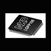
LPC2921_23_25 NXP Semiconductors, LPC2921_23_25 Datasheet - Page 31

LPC2921_23_25
Manufacturer Part Number
LPC2921_23_25
Description
The LPC2921/2923/2925 combine an ARM968E-S CPU core with two integrated TCMblocks operating at frequencies of up to 125 MHz, Full-speed USB 2
Manufacturer
NXP Semiconductors
Datasheet
1.LPC2921_23_25.pdf
(84 pages)
- Current page: 31 of 84
- Download datasheet (552Kb)
NXP Semiconductors
LPC2921_23_25_3
Product data sheet
6.13.3.1 Pin description
6.14.1 Functional description
6.14 Modulation and Sampling Control SubSystem (MSCSS)
Table 19.
[1]
The Modulation and Sampling Control Subsystem (MSCSS) in the LPC2921/2923/2925
includes four Pulse Width Modulators (PWMs), two 10-bit successive approximation
Analog-to-Digital Converters (ADCs) and two timers.
The key features of the MSCSS are:
The MSCSS contains Pulse Width Modulators (PWMs), Analog-to-Digital Converters
(ADCs) and timers.
Figure 5
communication with the AHB system bus. Two internal timers are dedicated to this
subsystem. MSCSS timer 0 can be used to generate start pulses for the ADCs and the
first PWM. The second timer (MSCSS timer 1) is used to generate ‘carrier’ signals for the
PWMs. These carrier patterns can be used, for example, in applications requiring current
control. Several other trigger possibilities are provided for the ADCs (external, cascaded
or following a PWM). The capture inputs of both timers can also be used to capture the
start pulse of the ADCs.
Symbol
I2C SCL0/1
I2C SDA0/1
•
•
•
•
•
•
•
•
•
•
•
•
Programmable clocks allow versatile rate control.
Bidirectional data transfer between masters and slaves.
Multi-master bus (no central master).
Arbitration between simultaneously transmitting masters without corruption of serial
data on the bus.
Serial clock synchronization allows devices with different bit rates to communicate via
one serial bus.
Serial clock synchronization can be used as a handshake mechanism to suspend and
resume serial transfer.
The I
All I
Note that the pins are not I
Two 10-bit, 400 ksample/s, 8-channel ADCs with 3.3 V inputs and various trigger-
start options.
Four 6-channel PWMs (Pulse Width Modulators) with capture and trap functionality.
Two dedicated timers to schedule and synchronize the PWMs and ADCs.
Quadrature encoder interface.
2
C-bus controllers support multiple address recognition and a bus monitor mode.
provides an overview of the MSCSS. An AHB-to-APB bus bridge takes care of
2
C-bus can be used for test and diagnostic purposes.
I
2
C-bus pins
Pin name
SCL0/1
SDA0/1
All information provided in this document is subject to legal disclaimers.
[1]
Rev. 03 — 14 April 2010
2
C-bus compliant open-drain pins.
Direction
I/O
I/O
ARM9 microcontroller with CAN, LIN, and USB
Description
I
I
2
2
C clock input/output
C data input/output
LPC2921/2923/2925
© NXP B.V. 2010. All rights reserved.
31 of 84
Related parts for LPC2921_23_25
Image
Part Number
Description
Manufacturer
Datasheet
Request
R
Part Number:
Description:
Arm9 Microcontroller With Can, Lin, And Usb Device
Manufacturer:
NXP Semiconductors
Datasheet:
Part Number:
Description:
(LPC2921 - LPC2925) ARM9 microcontroller
Manufacturer:
NXP Semiconductors
Datasheet:
Part Number:
Description:
NXP Semiconductors designed the LPC2420/2460 microcontroller around a 16-bit/32-bitARM7TDMI-S CPU core with real-time debug interfaces that include both JTAG andembedded trace
Manufacturer:
NXP Semiconductors
Datasheet:

Part Number:
Description:
NXP Semiconductors designed the LPC2458 microcontroller around a 16-bit/32-bitARM7TDMI-S CPU core with real-time debug interfaces that include both JTAG andembedded trace
Manufacturer:
NXP Semiconductors
Datasheet:
Part Number:
Description:
NXP Semiconductors designed the LPC2468 microcontroller around a 16-bit/32-bitARM7TDMI-S CPU core with real-time debug interfaces that include both JTAG andembedded trace
Manufacturer:
NXP Semiconductors
Datasheet:
Part Number:
Description:
NXP Semiconductors designed the LPC2470 microcontroller, powered by theARM7TDMI-S core, to be a highly integrated microcontroller for a wide range ofapplications that require advanced communications and high quality graphic displays
Manufacturer:
NXP Semiconductors
Datasheet:
Part Number:
Description:
NXP Semiconductors designed the LPC2478 microcontroller, powered by theARM7TDMI-S core, to be a highly integrated microcontroller for a wide range ofapplications that require advanced communications and high quality graphic displays
Manufacturer:
NXP Semiconductors
Datasheet:
Part Number:
Description:
The Philips Semiconductors XA (eXtended Architecture) family of 16-bit single-chip microcontrollers is powerful enough to easily handle the requirements of high performance embedded applications, yet inexpensive enough to compete in the market for hi
Manufacturer:
NXP Semiconductors
Datasheet:
Part Number:
Description:
The XA-S3 device is a member of Philips Semiconductors? XA(eXtended Architecture) family of high performance 16-bitsingle-chip microcontrollers
Manufacturer:
NXP Semiconductors
Datasheet:

Part Number:
Description:
The NXP BlueStreak LH75401/LH75411 family consists of two low-cost 16/32-bit System-on-Chip (SoC) devices
Manufacturer:
NXP Semiconductors
Datasheet:

Part Number:
Description:
The NXP LPC3130/3131 combine an 180 MHz ARM926EJ-S CPU core, high-speed USB2
Manufacturer:
NXP Semiconductors
Datasheet:

Part Number:
Description:
The NXP LPC3141 combine a 270 MHz ARM926EJ-S CPU core, High-speed USB 2
Manufacturer:
NXP Semiconductors

Part Number:
Description:
The NXP LPC3143 combine a 270 MHz ARM926EJ-S CPU core, High-speed USB 2
Manufacturer:
NXP Semiconductors

Part Number:
Description:
The NXP LPC3152 combines an 180 MHz ARM926EJ-S CPU core, High-speed USB 2
Manufacturer:
NXP Semiconductors


