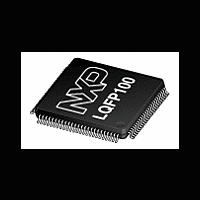
LPC2921_23_25 NXP Semiconductors, LPC2921_23_25 Datasheet - Page 20

LPC2921_23_25
Manufacturer Part Number
LPC2921_23_25
Description
The LPC2921/2923/2925 combine an ARM968E-S CPU core with two integrated TCMblocks operating at frequencies of up to 125 MHz, Full-speed USB 2
Manufacturer
NXP Semiconductors
Datasheet
1.LPC2921_23_25.pdf
(84 pages)
NXP Semiconductors
LPC2921_23_25_3
Product data sheet
6.10.1 USB device controller
6.8.6 EEPROM
6.9.1 DMA support for peripherals
6.9.2 Clock description
6.10 USB interface
6.9 General Purpose DMA (GPDMA) controller
EEPROM is a non-volatile memory mostly used for storing relatively small amounts of
data, for example for storing settings. It contains one 16 kB memory block and is
byte-programmable and byte-erasable.
The EEPROM can be accessed only through the flash controller.
The GPDMA controller allows peripheral-to-memory, memory-to-peripheral,
peripheral-to-peripheral, and memory-to-memory transactions. Each DMA stream
provides unidirectional serial DMA transfers for a single source and destination. For
example, a bidirectional port requires one stream for transmit and one for receives. The
source and destination areas can each be either a memory region or a peripheral, and
can be accessed through the same AHB master or one area by each master.
The GPDMA controls eight DMA channels with hardware prioritization. The DMA
controller interfaces to the system via two AHB bus masters, each with a full 32-bit data
bus width. DMA operations may be set up for 8-bit, 16-bit, and 32-bit data widths, and can
be either big-endian or little-endian. Incrementing or non-incrementing addressing for
source and destination are supported, as well as programmable DMA burst size. Scatter
or gather DMA is supported through the use of linked lists. This means that the source
and destination areas do not have to occupy contiguous areas of memory.
The GPDMA supports the following peripherals: SPI0/1/2 and UART0/1. The GPDMA can
access both embedded SRAM blocks, both TCMs, external static memory, and flash
memory.
The DMA controller is clocked by CLK_SYS_DMA derived from BASE_SYS_CLK, see
Section
The Universal Serial Bus (USB) is a 4-wire bus that supports communication between a
host and one or more (up to 127) peripherals. The bus supports hot plugging and dynamic
configuration of the devices. All transactions are initiated by the Host controller.
The LPC2921/2923/2925 USB interface includes a device controller with on-chip PHY for
device. Details on typical USB interfacing solutions can be found in
The device controller enables 12 Mbit/s data exchange with a USB Host controller. It
consists of a register interface, serial interface engine, endpoint buffer memory, and a
DMA controller. The serial interface engine decodes the USB data stream and writes data
to the appropriate endpoint buffer. The status of a completed USB transfer or error
condition is indicated via status registers. An interrupt is also generated if enabled. When
enabled, the DMA controller transfers data between the endpoint buffer and the on-chip
SRAM.
6.7.2.
All information provided in this document is subject to legal disclaimers.
Rev. 03 — 14 April 2010
ARM9 microcontroller with CAN, LIN, and USB
LPC2921/2923/2925
Section
© NXP B.V. 2010. All rights reserved.
10.2.
20 of 84


