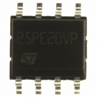
M25PE20-VMN6TP NUMONYX, M25PE20-VMN6TP Datasheet - Page 10

M25PE20-VMN6TP
Manufacturer Part Number
M25PE20-VMN6TP
Description
IC FLASH 2MBIT 75MHZ 8SOIC
Manufacturer
NUMONYX
Series
Forté™r
Datasheet
1.M25PE10-VMN6TP.pdf
(64 pages)
Specifications of M25PE20-VMN6TP
Format - Memory
FLASH
Memory Type
FLASH
Memory Size
2M (256K x 8)
Speed
75MHz
Interface
SPI, 3-Wire Serial
Voltage - Supply
2.7 V ~ 3.6 V
Operating Temperature
-40°C ~ 85°C
Package / Case
8-SOIC (3.9mm Width)
Cell Type
NOR
Density
2Mb
Access Time (max)
8ns
Interface Type
Serial (SPI)
Boot Type
Not Required
Address Bus
1b
Operating Supply Voltage (typ)
3.3V
Operating Temp Range
-40C to 85C
Package Type
SOIC N
Sync/async
Synchronous
Operating Temperature Classification
Industrial
Operating Supply Voltage (min)
2.7V
Operating Supply Voltage (max)
3.6V
Word Size
8b
Number Of Words
256K
Supply Current
8mA
Mounting
Surface Mount
Pin Count
8
Lead Free Status / RoHS Status
Lead free / RoHS Compliant
Other names
M25PE20-VMN6TPTR
Available stocks
Company
Part Number
Manufacturer
Quantity
Price
Company:
Part Number:
M25PE20-VMN6TP
Manufacturer:
MICRON
Quantity:
3 000
Company:
Part Number:
M25PE20-VMN6TP
Manufacturer:
Numonyx
Quantity:
16 500
Part Number:
M25PE20-VMN6TP
Manufacturer:
MICRON/美光
Quantity:
20 000
SPI modes
3
10/64
SPI modes
These devices can be driven by a microcontroller with its SPI peripheral running in either of
the two following modes:
●
●
For these two modes, input data is latched in on the rising edge of Serial Clock (C), and
output data is available from the falling edge of Serial Clock (C).
The difference between the two modes, as shown in
bus master is in Standby mode and not transferring data:
●
●
Figure 4.
1. The Write Protect or Top Sector Lock (W or TSL) signal should be driven, High or Low as appropriate.
Figure 4
device is selected at a time, so only one device drives the Serial Data output (Q) line at a
time, the other devices are high impedance. Resistors R (represented in
that the M25PE20 or M25PE10 is not selected if the Bus Master leaves the S line in the high
impedance state. As the Bus Master may enter a state where all inputs/outputs are in high
impedance at the same time (for example, when the Bus Master is reset), the clock line (C)
must be connected to an external pull-down resistor so that, when all inputs/outputs become
high impedance, the S line is pulled High while the C line is pulled Low (thus ensuring that S
and C do not become High at the same time, and so, that the t
The typical value of R is 100 kΩ , assuming that the time constant R*C
capacitance of the bus line) is shorter than the time during which the Bus Master leaves the
SPI bus in high impedance.
SPI interface with
(CPOL, CPHA) =
CS3
(0, 0) or (1, 1)
SPI Bus Master
CPOL=0, CPHA=0
CPOL=1, CPHA=1
C remains at 0 for (CPOL=0, CPHA=0)
C remains at 1 for (CPOL=1, CPHA=1)
shows an example of three devices connected to an MCU, on an SPI bus. Only one
CS2 CS1
Bus master and memory devices on the SPI bus
SDO
SDI
SCK
R
R
C Q D
S
SPI memory
device
W
or
TSL
V
CC
Reset
V
R
SS
C Q D
S
Figure
SPI memory
device
W
or
TSL
5, is the clock polarity when the
V
CC
SHCH
Reset
V
R
SS
requirement is met).
p
M25PE20, M25PE10
(C
C Q D
Figure
S
p
SPI memory
= parasitic
device
4) ensure
W
or
TSL
V
CC
Reset
AI13558b
V
V
V
SS
CC
SS


