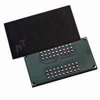
MT48H4M16LFB4-8 IT Micron Technology Inc, MT48H4M16LFB4-8 IT Datasheet - Page 16

MT48H4M16LFB4-8 IT
Manufacturer Part Number
MT48H4M16LFB4-8 IT
Description
IC SDRAM 64MBIT 125MHZ 54VFBGA
Manufacturer
Micron Technology Inc
Datasheet
1.MT48H4M16LFB4-10.pdf
(54 pages)
Specifications of MT48H4M16LFB4-8 IT
Format - Memory
RAM
Memory Type
Mobile SDRAM
Memory Size
64M (4M x 16)
Speed
125MHz
Interface
Parallel
Voltage - Supply
1.7 V ~ 1.9 V
Operating Temperature
-40°C ~ 85°C
Package / Case
54-VFBGA
Lead Free Status / RoHS Status
Lead free / RoHS Compliant
READs
shown in Figure 8.
vided with the READ command, and auto precharge is
either enabled or disabled for that burst access. If auto
precharge is enabled, the row being accessed is pre-
charged at the completion of the burst. For the generic
READ commands used in the following illustrations,
auto precharge is disabled.
from the starting column address will be available fol-
lowing the CAS latency after the READ command.
Each subsequent data-out element will be valid by the
next positive clock edge. Figure 5, CAS Latency, on
page 10, shows general timing for each possible CAS
latency setting.
commands have been initiated, the DQ will go High-Z.
A full-page burst will continue until terminated. (At the
end of the page, it will wrap to column 0 and continue.)
subsequent READ command, and data from a fixed-
length READ burst may be immediately followed by
data from a READ command. In either case, a continu-
ous flow of data can be maintained. The first data ele-
ment from the new burst follows either the last
element of a completed burst or the last desired data
element of a longer burst that is being truncated. The
new READ command should be issued x cycles before
the clock edge at which the last desired data element is
valid, where x equals the CAS latency minus one.
Bursts, on page 17 for CAS latencies of two and three;
data element n + 3 is either the last of a burst of four or
the last desired of a longer burst. The 64Mb SDRAM
uses a pipelined architecture and therefore does not
require the 2n rule associated with a prefetch architec-
ture. A READ command can be initiated on any clock
cycle following a previous READ command. Full-speed
random read accesses can be performed to the same
bank, as shown in Figure 11, Random READ Accesses,
on page 17, or each subsequent READ may be per-
formed to a different bank.
pdf: 09005aef80a63953, source: 09005aef808a7edc
Y25L_64Mb_2.fm - Rev. E 11/04 EN
READ bursts are initiated with a READ command, as
The starting column and bank addresses are pro-
During READ bursts, the valid data-out element
Upon completion of a burst, assuming no other
Data from any READ burst may be truncated with a
This is shown in Figure 10, Consecutive READ
16
subsequent WRITE command, and data from a fixed-
length READ burst may be immediately followed by
data from a WRITE command (subject to bus turn-
around limitations). The WRITE burst may be initiated
on the clock edge immediately following the last (or
last desired) data element from the READ burst, pro-
vided that I/O contention can be avoided. In a given
system design, there may be a possibility that the
device driving the input data will go Low-Z before the
SDRAM DQ go High-Z. In this case, at least a single-
cycle delay should occur between the last read data
and the WRITE command.
Data from any READ burst may be truncated with a
A9, A11
BA0,1
Micron Technology, Inc., reserves the right to change products or specifications without notice.
A0-A7
CAS#
RAS#
WE#
A10
CLK
CKE
CS#
Figure 9: READ Command
HIGH
DISABLE AUTO PRECHARGE
ENABLE AUTO PRECHARGE
MOBILE SDRAM
©2003 Micron Technology, Inc. All rights reserved.
COLUMN
ADDRESS
ADDRESS
BANK
64Mb: x16
DON’T CARE


