CY7C135-25JXC Cypress Semiconductor Corp, CY7C135-25JXC Datasheet - Page 2
CY7C135-25JXC
Manufacturer Part Number
CY7C135-25JXC
Description
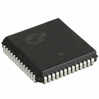
IC SRAM 32KBIT 25NS 52PLCC
Manufacturer
Cypress Semiconductor Corp
Datasheet
1.CY7C135-15JXC.pdf
(12 pages)
Specifications of CY7C135-25JXC
Format - Memory
RAM
Memory Type
SRAM - Dual Port, Asynchronous
Memory Size
32K (4K x 8)
Speed
25ns
Interface
Parallel
Voltage - Supply
4.5 V ~ 5.5 V
Operating Temperature
0°C ~ 70°C
Package / Case
52-PLCC
Density
32Kb
Access Time (max)
25ns
Sync/async
Asynchronous
Architecture
Not Required
Clock Freq (max)
Not RequiredMHz
Operating Supply Voltage (typ)
5V
Address Bus
12b
Package Type
PLCC
Operating Temp Range
0C to 70C
Number Of Ports
2
Supply Current
180mA
Operating Supply Voltage (min)
4.5V
Operating Supply Voltage (max)
5.5V
Operating Temperature Classification
Commercial
Mounting
Surface Mount
Pin Count
52
Word Size
8b
Number Of Words
4K
Lead Free Status / RoHS Status
Lead free / RoHS Compliant
Available stocks
Company
Part Number
Manufacturer
Quantity
Price
Company:

Part Number:
CY7C135-25JXC
Manufacturer:
Cypress Semiconductor Corp
Quantity:
10 000


Selection Guide
Pin Configurations
Figure 1. Pin Diagram - CY7C135/135A (Top View)
Pin Definitions
Document #: 38-06038 Rev. *D
Maximum Access Time
Maximum Operating Current
Maximum Standby Current for
I
A
CE
OE
R/W
SEM
(CY7C1342
only)
SB1
0L–11L
L
L
Left Port
L
L
I/O
I/O
I/O
I/O
A
A
A
A
A
A
A
A
A
1L
2L
3L
4L
5L
6L
7L
8L
9L
0L
1L
2L
3L
8
9
10
11
12
13
14
15
16
17
18
19
20
Parameter
21 22 23 24 25 26 27 28 29 30 31 32 33
A
CE
OE
R/W
SEM
(CY7C1342
only)
7 6 5 4 3 2
0R–11R
Right Port
R
R
R
R
7C135/135A
1
Commercial
Commercial
52 51 50 49 48 47
Address Lines
Chip Enable
Output Enable
Read/Write Enable
Semaphore Enable. When asserted LOW, allows access to eight semaphores. The three least
significant bits of the address lines determines which semaphore to write or read. The I/O
is used when writing to a semaphore. Semaphores are requested by writing a 0 into the
respective location.
46
45
44
43
42
41
40
39
38
37
36
35
34
7C1342-15
7C135-15
OE
A
A
A
A
A
A
A
A
A
A
NC
I/O
0R
1R
2R
3R
4R
5R
6R
7R
8R
9R
220
7R
R
15
60
7C1342-20
7C135-20
190
20
50
Figure 2. Pin Diagram - CY7C1342 (Top View)
7C135/135A-25
Description
7C1342-25
I/O
I/O
I/O
I/O
A
A
A
A
A
A
A
A
A
1L
2L
3L
4L
5L
6L
7L
8L
9L
0L
1L
2L
3L
180
25
40
8
9
10
11
12
13
14
15
16
17
18
19
20
21 22 23 24 25 26 27 28 29 30 31 32 33
7 6 5 4 3 2
7C1342-35
7C135-35
CY7C135, CY7C135A
7C1342
160
1
35
30
52 51 50 49 48 47
7C1342-55
7C135-55
CY7C1342
46
45
44
43
42
41
40
39
38
37
36
35
34
160
55
30
OE
A
A
A
A
A
A
A
A
A
A
NC
I/O
Page 2 of 12
0R
1R
2R
3R
4R
5R
6R
7R
8R
9R
7R
R
0
Unit
mA
mA
ns
pin
[+] Feedback
Related parts for CY7C135-25JXC
Image
Part Number
Description
Manufacturer
Datasheet
Request
R

Part Number:
Description:
IC SRAM 32KBIT 15NS 52PLCC
Manufacturer:
Cypress Semiconductor Corp
Datasheet:

Part Number:
Description:
Manufacturer:
Cypress Semiconductor Corp
Datasheet:
Part Number:
Description:
Manufacturer:
Cypress Semiconductor Corp
Datasheet:

Part Number:
Description:
CY7C135-25JXI
Manufacturer:
Cypress Semiconductor Corp
Datasheet:
Part Number:
Description:
Manufacturer:
Cypress Semiconductor Corp
Datasheet:
Part Number:
Description:
Manufacturer:
Cypress Semiconductor Corp
Datasheet:
Part Number:
Description:
Manufacturer:
Cypress Semiconductor Corp
Datasheet: