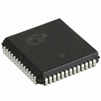
CY7C135-25JXC Cypress Semiconductor Corp, CY7C135-25JXC Datasheet - Page 5

CY7C135-25JXC
Manufacturer Part Number
CY7C135-25JXC
Description
IC SRAM 32KBIT 25NS 52PLCC
Manufacturer
Cypress Semiconductor Corp
Datasheet
1.CY7C135-15JXC.pdf
(12 pages)
Specifications of CY7C135-25JXC
Format - Memory
RAM
Memory Type
SRAM - Dual Port, Asynchronous
Memory Size
32K (4K x 8)
Speed
25ns
Interface
Parallel
Voltage - Supply
4.5 V ~ 5.5 V
Operating Temperature
0°C ~ 70°C
Package / Case
52-PLCC
Density
32Kb
Access Time (max)
25ns
Sync/async
Asynchronous
Architecture
Not Required
Clock Freq (max)
Not RequiredMHz
Operating Supply Voltage (typ)
5V
Address Bus
12b
Package Type
PLCC
Operating Temp Range
0C to 70C
Number Of Ports
2
Supply Current
180mA
Operating Supply Voltage (min)
4.5V
Operating Supply Voltage (max)
5.5V
Operating Temperature Classification
Commercial
Mounting
Surface Mount
Pin Count
52
Word Size
8b
Number Of Words
4K
Lead Free Status / RoHS Status
Lead free / RoHS Compliant
Available stocks
Company
Part Number
Manufacturer
Quantity
Price
Company:
Part Number:
CY7C135-25JXC
Manufacturer:
Cypress Semiconductor Corp
Quantity:
10 000
Switching Characteristics
Document #: 38-06038 Rev. *D
t
t
t
t
t
t
t
t
t
t
t
t
t
t
t
t
t
t
t
t
t
t
t
t
t
t
Notes
RC
AA
OHA
ACE
DOE
LZOE
HZOE
LZCE
HZCE
PU
PD
WC
SCE
AW
HA
SA
PWE
SD
HD
HZWE
LZWE
WDD
DDD
SOP
SWRD
SPS
6. Test conditions assume signal transition time of 3 ns or less, timing reference levels of 1.5V, input pulse levels of 0 to 3.0V, and output loading of the specified I
7. At any given temperature and voltage condition for any given device, t
8. Test conditions used are Load 3.
9. This parameter is guaranteed but not tested.
10. For information on port-to-port delay through RAM cells from writing port to reading port, refer to
11. Semaphore timing applies only to CY7C1342.
Read Cycle
Write Cycle
Semaphore Timing
Parameter
[9]
[9]
and 30 pF load capacitance.
[10]
[10]
[7,8,9]
[7,8,9]
[7,8,9]
[7,8,9]
[8,9]
[8,9]
Read Cycle Time
Address to Data Valid
Output Hold From Address Change
CE LOW to Data Valid
OE LOW to Data Valid
OE Low to Low Z
OE HIGH to High Z
CE LOW to Low Z
CE HIGH to High Z
CE LOW to Power Up
CE HIGH to Power Down
Write Cycle Time
CE LOW to Write End
Address Setup to Write End
Address Hold from Write End
Address Setup to Write Start
Write Pulse Width
Data Setup to Write End
Data Hold from Write End
R/W LOW to High Z
R/W HIGH to Low Z
Write Pulse to Data Delay
Write Data Valid to Read Data Valid
SEM Flag Update Pulse
(OE or SEM)
SEM Flag Write to Read Time
SEM Flag Contention Window
[11]
Description
Over the Operating Range
7C1342-15
Min
7C135-15
15
15
12
12
12
10
10
5
5
3
3
3
0
2
0
0
3
HZCE
Max
15
10
10
10
15
10
30
25
15
is less than t
[6]
7C1342-20
Min
7C135-20
20
20
15
15
15
13
10
3
3
3
0
2
0
0
3
5
5
LZCE
Max
20
20
13
13
13
20
13
40
30
and t
Figure
HZOE
7C135A-25
7C1342-25
Min
7C135-25
25
25
20
20
20
15
10
3
3
3
0
2
0
0
3
5
5
6.
is less than t
Max
25
15
50
25
15
15
25
15
30
LZOE
7C1342-35
CY7C135, CY7C135A
Min
7C135-35
35
35
30
30
25
15
15
3
3
3
0
2
0
0
3
5
5
.
Max
35
35
20
20
20
35
20
60
35
7C1342-55
Min
7C135-55
55
55
50
50
50
25
15
3
3
3
0
2
0
0
3
5
5
CY7C1342
Max
55
55
25
25
25
55
25
70
40
Page 5 of 12
Unit
OL
ns
ns
ns
ns
ns
ns
ns
ns
ns
ns
ns
ns
ns
ns
ns
ns
ns
ns
ns
ns
ns
ns
ns
ns
ns
ns
/I
OH
[+] Feedback


