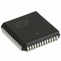
CY7C135-25JXC Cypress Semiconductor Corp, CY7C135-25JXC Datasheet - Page 8

CY7C135-25JXC
Manufacturer Part Number
CY7C135-25JXC
Description
IC SRAM 32KBIT 25NS 52PLCC
Manufacturer
Cypress Semiconductor Corp
Datasheet
1.CY7C135-15JXC.pdf
(12 pages)
Specifications of CY7C135-25JXC
Format - Memory
RAM
Memory Type
SRAM - Dual Port, Asynchronous
Memory Size
32K (4K x 8)
Speed
25ns
Interface
Parallel
Voltage - Supply
4.5 V ~ 5.5 V
Operating Temperature
0°C ~ 70°C
Package / Case
52-PLCC
Density
32Kb
Access Time (max)
25ns
Sync/async
Asynchronous
Architecture
Not Required
Clock Freq (max)
Not RequiredMHz
Operating Supply Voltage (typ)
5V
Address Bus
12b
Package Type
PLCC
Operating Temp Range
0C to 70C
Number Of Ports
2
Supply Current
180mA
Operating Supply Voltage (min)
4.5V
Operating Supply Voltage (max)
5.5V
Operating Temperature Classification
Commercial
Mounting
Surface Mount
Pin Count
52
Word Size
8b
Number Of Words
4K
Lead Free Status / RoHS Status
Lead free / RoHS Compliant
Available stocks
Company
Part Number
Manufacturer
Quantity
Price
Company:
Part Number:
CY7C135-25JXC
Manufacturer:
Cypress Semiconductor Corp
Quantity:
10 000
Switching Waveforms
Document #: 38-06038 Rev. *D
Notes
20. CE = HIGH for the duration of the above timing (both write and read cycle).
21. I/O
22. Semaphores are reset (available to both ports) at cycle start.
23. If t
A
A
A
SPS
0L
0R
0R
0
SEM
SEM
–A
R/W
SEM
I/O
–A
R/W
R/W
–A
= I/O
OE
is violated, it is guaranteed that only one side gains access to the semaphore.
2
2L
0
2R
R
R
L
L
0L
= LOW (request semaphore); CE
Figure 10. Timing Diagram of Semaphore Contention (CY7C1342 Only)
Figure 9. Semaphore Read After Write Timing, Either Side (CY7C1342 only)
t
SA
(continued)
VALID ADDRESS
t
AW
WRITE CYCLE
t
R
t
PWE
SCE
= CE
t
SD
DATA
t
MATCH
SPS
MATCH
L
= HIGH.
t
IN
HA
VALID
t
HD
t
SWRD
t
SOP
t
SOP
READ CYCLE
VALID ADDRESS
t
AA
t
DOE
t
ACE
DATA
CY7C135, CY7C135A
[21, 22, 23]
OUT
[20]
VALID
t
OHA
CY7C1342
Page 8 of 12
[+] Feedback


