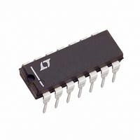
LT1105IN Linear Technology, LT1105IN Datasheet - Page 15

LT1105IN
Manufacturer Part Number
LT1105IN
Description
IC OFFLINE SWIT CM HV 14DIP
Manufacturer
Linear Technology
Datasheet
1.LT1105CN8PBF.pdf
(32 pages)
Specifications of LT1105IN
Output Isolation
Isolated
Frequency Range
20 ~ 200kHz
Voltage - Input
7 ~ 30 V
Voltage - Output
20V
Power (watts)
100W
Operating Temperature
-40°C ~ 125°C
Package / Case
14-DIP (0.300", 7.62mm)
Lead Free Status / RoHS Status
Contains lead / RoHS non-compliant
Available stocks
Company
Part Number
Manufacturer
Quantity
Price
Part Number:
LT1105IN
Manufacturer:
LINEAR/凌特
Quantity:
20 000
Part Number:
LT1105IN#PBF
Manufacturer:
LINEAR/凌特
Quantity:
20 000
Company:
Part Number:
LT1105IN8#PBF
Manufacturer:
LINEAR
Quantity:
29
Part Number:
LT1105IN8#PBF
Manufacturer:
LINEAR/凌特
Quantity:
20 000
OPER
Control of output voltage is obtained by using the output
of a voltage sensing error amplifier to set current trip level.
This technique has several advantages. First, it has imme-
diate response to input voltage variations, unlike ordinary
switchers which have notoriously poor line transient re-
sponse. Second, it reduces the 90 phase shift at
midfrequencies in the transformer. This greatly simplifies
closed-loop frequency compensation under widely vary-
ing input voltage or output load conditions. Finally, it
allows simple pulse-by-pulse current limiting to provide
maximum switch protection under output overload or
short-circuit conditions.
A start-up loop with hysteresis allows the IC supply
voltage to be bootstrapped from an extra primary side
winding on the power transformer. From 0V to 16V on V
the LT1105 is in prestart mode and total input current is
typically 200 A. Above 16V, up to 30V, the 6V regulator
that biases the internal circuitry and the externally avail-
able 5V and 15V regulators are turned on. The internal
circuitry remains biased on until V
the part returns to prestart mode. Output switching stops
when the 15V gate bias reference is less than 10V corre-
sponding to V
The oscillator provides the basic clock for all internal
timing. Frequency is adjustable to 200kHz with one exter-
nal capacitor from OSC to ground. The oscillator turns on
the output switch via the logic and driver circuitry.
The LT1105 is designed to drive the gate of an external
power FET in common source configuration. The drivers
and the 1A maximum totem-pole output stage are biased
from the 15V gate bias reference. Special drive detection
circuity senses the gate bias reference voltage and pre-
vents the output switch from turning on if this voltage is
less than 10V or greater than 20V. Break-Before-Make
action of 200ns is built into each switch edge to eliminate
cross conduction currents.
Switch current is sensed externally through a precision,
power resistor. This allows for greater flexibility in switch
current and output power than allowed by the LT1103. The
voltage across the sense resistor is fed into the I
amplified to trip the comparator and turn off the switch
according to the V
ATIO
IN
of about 12V.
U
C
pin control voltage. A blanking circuit
IN
drops below 7V and
LIM
pin and
IN
,
suppresses the output of the current limit comparator for
500ns at the beginning of each switch cycle. This prevents
false tripping of the comparator due to current spikes
caused by external parasitic capacitance and diode stored
charge.
A 4.5V Zener-based reference biases the positive input of
the sampling error amplifier. The negative input (FB) is
used for output voltage sensing. The sampling error
amplifier allows the LT1105 to operate in fully isolated
flyback mode by regulating the flyback voltage of the
bootstrap winding. The leakage inductance spike at the
leading edge of the flyback waveform is ignored with a
blanking circuit. The flyback waveform is directly propor-
tional to the output voltage in the transformer coupled
flyback topology. Output voltages are fully floating up to
the breakdown voltage of the transformer windings. Mul-
tiple floating outputs are easily obtained with additional
windings.
The error signal developed at the comparator input is
brought out externally. The V
including frequency compensation, current limit adjust-
ment and total regulator shutdown. During normal opera-
tion, this pin sits at a voltage between 1.2V (low output
current) and 4.4V (high output current). The error ampli-
fier is a current output (g
externally clamped for adjusting current limit. Switch duty
cycle goes to zero if the V
a diode, placing the LT1105 in an idle mode. Pulling the V
pin below 0.15V causes total regulator shutdown and
places the LT1105 in prestart mode.
The SS pin implements soft-start with one external capaci-
tor to ground. The internal pull-up current and clamp
transistor limit the voltage at V
the voltage at the SS pin, thereby controlling the rate of rise
of switch current in the regulator. The SS pin is reset to 0V
when the LT1105 is in prestart mode.
A final protection feature includes overvoltage lockout
monitoring of the main supply voltage on the OVLO pin. If
the OVLO pin is greater than 2.5V, the output switch is
prevented from turning on. This function can be disabled
by grounding the OVLO pin.
C
m
pin is pulled to ground through
) type, so this voltage can be
LT1103/LT1105
C
C
to one diode drop above
pin has three functions
15
C


