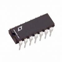
LT1105IN Linear Technology, LT1105IN Datasheet - Page 5

LT1105IN
Manufacturer Part Number
LT1105IN
Description
IC OFFLINE SWIT CM HV 14DIP
Manufacturer
Linear Technology
Datasheet
1.LT1105CN8PBF.pdf
(32 pages)
Specifications of LT1105IN
Output Isolation
Isolated
Frequency Range
20 ~ 200kHz
Voltage - Input
7 ~ 30 V
Voltage - Output
20V
Power (watts)
100W
Operating Temperature
-40°C ~ 125°C
Package / Case
14-DIP (0.300", 7.62mm)
Lead Free Status / RoHS Status
Contains lead / RoHS non-compliant
Available stocks
Company
Part Number
Manufacturer
Quantity
Price
Part Number:
LT1105IN
Manufacturer:
LINEAR/凌特
Quantity:
20 000
Part Number:
LT1105IN#PBF
Manufacturer:
LINEAR/凌特
Quantity:
20 000
Company:
Part Number:
LT1105IN8#PBF
Manufacturer:
LINEAR
Quantity:
29
Part Number:
LT1105IN8#PBF
Manufacturer:
LINEAR/凌特
Quantity:
20 000
ELECTRICAL CHARACTERISTICS
V
SYMBOL
The
temperature range.
Note 1: Absolute Maximum Ratings are those values beyond which the life
of a device may be impaired.
Note 2: The OVLO pin is clamped with a 5.5V Zener and can sink a
maximum input current of 1mA.
Note 3: FB input bias current changes as a function of the V
Rate of change of FB input bias current is 11 A/V of change on V
including a resistor in series with the FB pin, load regulation can be set
to zero.
TYPICAL PERFORMANCE CHARACTERISTICS
IN
25
20
15
10
= 20V, V
5
0
denotes specifications which apply over the full operating
0
Supply Current vs Input Voltage
I
SHUT
PARAMETER
Switch Output Low Level
(LT1105)
Rise Time (LT1105)
Fall Time (LT1105)
I
Low Switch Drive Lockout
Threshold
High Switch Drive Lockout
Threshold
5
LIM
C
= 0.85V, OVLO = 0V, V
Threshold Voltage (LT1105)
INPUT VOLTAGE (V)
10
I
START
25°C
15
20
W
25
LT1103 G01
SW
U
30
Open, T
CONDITONS
I
I
C
C
Duty Cycle = 25% (Note 5)
Measured at V
Measured at 15V Gate Bias Reference (LT1105)
Measured at V
Measured at 15V Gate Bias Reference (LT1105)
SW
SW
L
L
= 1000pF
= 1000pF
A
= 200mA
= 750mA
500
400
250
200
100
450
350
300
150
50
25 C, unless otherwise noted.
0
C
Start-Up Supply Current vs
Input Voltage
0
pin voltage.
SW
SW
C
. By
3
(LT1103)
(LT1103)
INPUT VOLTAGE (V)
6
125 C
–55 C
Note 4: Current limit on V
DC > 35% due to internal slope compensation circuity. The LT1103 switch
current limit is given by I
Note 5: The current limit threshold voltage is constant for DC < 35% and
decreases for DC > 35% due to internal slope compensation circuitry. The
LT1105 switch current limit threshold voltage is given by V
(1.7 – DC) above 35% duty cycle.
9
12
25 C
LT1103 G02
15
LIM
SW
= 1.76 (1.536 – DC) above 35% duty cycle.
is constant for DC < 35% and decreases for
18
12
22
21
20
19
17
16
15
14
13
Quiescent Supply Current vs
Input Voltage
0
5
LT1103/LT1105
17.0
MIN
300
9.0
10
INPUT VOLTAGE (V)
15
0.25
0.75
18.5
TYP
375
9.5
50
20
20
MAX
0.50
1.50
10.5
20.0
25
450
LIM
= 0.225
30
125°C
25°C
–55°C
35
LT1103 G03
UNIT
5
mV
ns
ns
40
V
V
V
V


