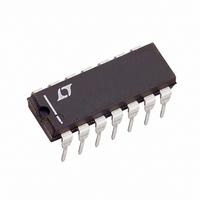
LT1105IN Linear Technology, LT1105IN Datasheet - Page 25

LT1105IN
Manufacturer Part Number
LT1105IN
Description
IC OFFLINE SWIT CM HV 14DIP
Manufacturer
Linear Technology
Datasheet
1.LT1105CN8PBF.pdf
(32 pages)
Specifications of LT1105IN
Output Isolation
Isolated
Frequency Range
20 ~ 200kHz
Voltage - Input
7 ~ 30 V
Voltage - Output
20V
Power (watts)
100W
Operating Temperature
-40°C ~ 125°C
Package / Case
14-DIP (0.300", 7.62mm)
Lead Free Status / RoHS Status
Contains lead / RoHS non-compliant
Available stocks
Company
Part Number
Manufacturer
Quantity
Price
Part Number:
LT1105IN
Manufacturer:
LINEAR/凌特
Quantity:
20 000
Part Number:
LT1105IN#PBF
Manufacturer:
LINEAR/凌特
Quantity:
20 000
Company:
Part Number:
LT1105IN8#PBF
Manufacturer:
LINEAR
Quantity:
29
Part Number:
LT1105IN8#PBF
Manufacturer:
LINEAR/凌特
Quantity:
20 000
APPLICATIONS
where N is the transformer turns ratio of secondary to
primary and DC is the duty cycle. This formula can be
rewritten in terms of duty cycle as:
It is important to define the full range of input voltage, the
range of output loading conditions and the regulation
requirements for a design. Duty cycle should be calculated
for both minimum and maximum input voltage.
In many applications, N can vary over a wide range without
degrading performance. If maximum output power is
desired, N can be optimized:
where
In the isolated flyback mode, the LT1103/LT1105 sense
and regulate the transformer primary voltage V
“switch off” time. The secondary output voltage will be
regulated if V
This allows duty cycle for an isolated flyback converter to
be rewritten as:
An important transformer parameter to be determined is
the primary inductance L
is a trade-off between core size, regulation requirements,
leakage inductance effects and magnetizing current I.
Magnetizing current is the difference between the primary
current at the start of “switch on” time and the current at
Vf = Forward voltage of the output diode
V
V
voltage.
DC =
N
DC = Duty Cycle =
V
M
SNUB
PRI
OPT
= Maximum switch voltage
=
= Snubber clamp level – primary flyback
V
=
OUT
V
OUT
PRI
V – V
V
M
OUT
N
is regulated. V
N • V
U
Vf
V
IN MAX
OUT
IN
V
PRI
INFORMATION
PRI
U
V
PRI
. The value of this inductance
Vf
– V
V
PRI
IN
SNUB
is related to V
W
U
PRI
OUT
during
by:
the end of “switch on” time. If maximum output power is
needed, a reasonable starting value is found by assigning
LT1103 and set by the external FET rating used with the
LT1105). With this design approach, L
If maximum output power is not required, then I can be
increased which results in lower primary inductance and
smaller magnetics. Maximum output power with an isolated
flyback converter is defined by the primary flyback voltage
and the peak allowed switch current and is limited to:
where
Peak primary current is used to determine core size for the
transformer and is found from:
A second consideration on primary inductance is the
transition point from continuous mode to discontinuous
mode. At light loads, the flyback pulse across the primary
will drop to zero before the end of “switch off” time. The
load current at which this starts to occur can be calculated
from:
The forward converter as shown below is another
transformer-based topology that converts one voltage to
either a higher or a lower voltage.
I a value of 20% of the peak switch current (2A for the
R = Total “switch” on resistance
I
E = Overall efficiency 75%
P
I
I
P
PRI
OUT(TRANSITION)
L
OUT(MAX)
PRI
= Maximum switch current
V
( I)(f) 1
OUT
E V
V
I
OUT
V
PRI
IN
PRI
V
PRI
V
V
PRI
V
V
IN
V
V
PRI
PRI
IN
IN
LT1103/LT1105
V
V
V
IN P
IN
IN
V
PRI
I –
2
2V
•
PRI
2
V
2
I
OUT
IN
I
is defined as:
2
– Ip R E
f L
25
2
PRI


