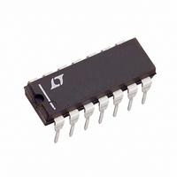
LT1105IN Linear Technology, LT1105IN Datasheet - Page 21

LT1105IN
Manufacturer Part Number
LT1105IN
Description
IC OFFLINE SWIT CM HV 14DIP
Manufacturer
Linear Technology
Datasheet
1.LT1105CN8PBF.pdf
(32 pages)
Specifications of LT1105IN
Output Isolation
Isolated
Frequency Range
20 ~ 200kHz
Voltage - Input
7 ~ 30 V
Voltage - Output
20V
Power (watts)
100W
Operating Temperature
-40°C ~ 125°C
Package / Case
14-DIP (0.300", 7.62mm)
Lead Free Status / RoHS Status
Contains lead / RoHS non-compliant
Available stocks
Company
Part Number
Manufacturer
Quantity
Price
Part Number:
LT1105IN
Manufacturer:
LINEAR/凌特
Quantity:
20 000
Part Number:
LT1105IN#PBF
Manufacturer:
LINEAR/凌特
Quantity:
20 000
Company:
Part Number:
LT1105IN8#PBF
Manufacturer:
LINEAR
Quantity:
29
Part Number:
LT1105IN8#PBF
Manufacturer:
LINEAR/凌特
Quantity:
20 000
APPLICATIONS
voltage, the secondary voltage, the bias voltage and the
winding currents are indicated in the figures found on the
following page for both continuous and discontinuous
modes of operation.
When the switch “turns on,” the primary winding sees the
input voltage and the secondary and bias windings go to
negative voltages as a function of the turns ratio. Current
builds in the primary winding as the transformer stores
energy. When the switch “turns off,” the voltage across
the switch flies back to a clamp level as defined by a
snubber network until the energy in the leakage induc-
tance of the primary dissipates. Leakage inductance is one
of the main parasitic elements in a flux-sensed converter
and is modeled as an inductor in series with the primary
and secondary of the transformer. These parasitic induc-
tances contribute to changes in the bias winding voltage
and thus the output voltage with increasing load current.
The energy stored in the transformer transfers through the
secondary and bias windings during “switch off” time.
Ideally, the voltage across the bias winding is set by the DC
output voltage, the forward voltage of the output diode,
and the turns ratio of the transformer after the energy in
the leakage inductance spike of the primary is dissipated.
This relationship holds until the energy in the transformer
drops to zero (discontinuous mode) or the switch turns on
again (continuous mode). Either case results in the volt-
age across the secondary and bias windings decreasing
V
BIAS
V
IN
L(Ik
PRI
S1
)
1:N1
1:N
Simplified Flyback Converter
U
L(lk
N = TURNS RATIO FROM SECONDARY TO PRIMARY.
N1 = TURNS RATIO FROM SECONDARY TO BIAS.
N2 = N/N1
L(lk
L(lk
R = PARASITIC WINDING, DIODE AND OUTPUT
SEC
PRI
SEC
CAPACITOR RESISTANCE.
)
INFORMATION
) = PRIMARY LEAKAGE INDUCTANCE.
) = SECONDARY LEAKAGE INDUCTANCE.
U
R
D1
W
C1
V
COMMON
OUT
LT1103 AI01
U
to zero or changing polarity. Therefore, the voltage on the
bias winding is only valid as a representation of the output
voltage while the secondary is delivering current.
Although the bias winding flyback voltage is a representa-
tion of the output voltage, its voltage is not constant. For
a brief period following the leakage inductance spike, the
bias winding flyback voltage decreases due to nonlinearities
and parasitics present in the transformer. Following this
nonlinear behavior is a period where the bias winding
flyback voltage decreases linearly. This behavior is easily
explained. Current flow in the secondary decreases lin-
early at a rate determined by the voltage across the
secondary and the inductance of the secondary. The
parasitic secondary leakage inductance appears as an
impedance in series with the secondary winding. In addi-
tion, parasitic resistances exist in the secondary winding,
the output diode and the output capacitor. These imped-
ances can be combined to form a lumped sum equivalent
and which cause a voltage drop as secondary current
flows. This voltage drop is coupled from the secondary to
the bias winding flyback voltage and becomes more sig-
nificant as the output is loaded more heavily. This voltage
drop is largest at the beginning of “switch off” time and
smallest just prior to either all transformer energy being
depleted or the switch turning on again.
The best representation of the output voltage is just prior
to either all transformer energy being used up and the bias
winding voltage collapsing to zero or just prior to the
switch turning on again and the bias winding going
negative. This point in time also represents the smallest
forward voltage for the output diode. It is possible to
redefine the relationship between the secondary winding
voltage and the bias winding voltage as:
where Vf is the forward voltage of the output diode, I is the
current flowing in the secondary, R
equivalent secondary parasitic impedance and N1 is the
transformer turns ratio from the secondary to the bias
winding. It is apparent that even though the above point in
V
BIAS
V
OUT
N1
Vf I • R
P
LT1103/LT1105
P
is the lumped sum
21


