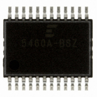
CS5460A-BSZ Cirrus Logic Inc, CS5460A-BSZ Datasheet - Page 27

CS5460A-BSZ
Manufacturer Part Number
CS5460A-BSZ
Description
IC ENERGY METERING 1PHASE 24SSOP
Manufacturer
Cirrus Logic Inc
Datasheet
1.CS5460A-BSZ.pdf
(54 pages)
Specifications of CS5460A-BSZ
Package / Case
24-SSOP
Input Impedance
30 KOhm
Measurement Error
0.1%
Voltage - I/o High
0.8V
Voltage - I/o Low
0.2V
Current - Supply
2.9mA
Voltage - Supply
4.75 V ~ 5.25 V
Operating Temperature
-40°C ~ 85°C
Mounting Type
Surface Mount
Meter Type
Single Phase
Output Voltage Range
2.4 V to 2.6 V
Output Current
1 uA
Input Voltage Range
2.4 V to 2.6 V
Input Current
25 nA
Power Dissipation
500 mW
Operating Temperature Range
- 40 C to + 85 C
Mounting Style
SMD/SMT
Ic Function
Single Phase Bi-directional Power / Energy IC
Brief Features
On-Chip Functions, AC Or DC System Calibration, Power Supply Monitor
Supply Voltage Range
3.3V To 5V
Rohs Compliant
Yes
Lead Free Status / RoHS Status
Lead free / RoHS Compliant
For Use With
CDB5460AU - EVALUATION BOARD FOR CS5460A
Lead Free Status / Rohs Status
Lead free / RoHS Compliant
Other names
598-1094-5
Available stocks
Company
Part Number
Manufacturer
Quantity
Price
Company:
Part Number:
CS5460A-BSZ
Manufacturer:
CIRRUS
Quantity:
2
Company:
Part Number:
CS5460A-BSZR
Manufacturer:
CIRRUS
Quantity:
8 000
Part Number:
CS5460A-BSZR
Manufacturer:
CIRRUS
Quantity:
20 000
that the Energy Register is read at least once in ev-
ery 5 second span.
3.5 Oscillator Characteristics
XIN and XOUT are the input and output, respec-
tively, of an inverting amplifier to provide oscillation
and can be configured as an on-chip oscillator, as
shown in Figure 15. The oscillator circuit is de-
signed to work with a quartz crystal or a ceramic
resonator. To reduce circuit cost, two load capaci-
tors C1 are integrated in the device, one between
XIN and DGND, one between XOUT and DGND.
Lead lengths should be minimized to reduce stray
capacitance.
To drive the device from an external clock source,
XOUT should be left unconnected while XIN is
driven by the external circuitry. There is an amplifi-
er between XIN and the digital section which pro-
vides CMOS level signals. This amplifier works
with sinusoidal inputs so there are no problems
with slow edge times.
The CS5460A can be driven by a clock ranging
from 2.5 to 20 MHz. The K divider must be set to
the appropriate value such that MCLK/K will be be-
tween 2.5 MHz and 5 MHz. The K divider value is
set with the K[3:0] bits in the Configuration Regis-
ter. As an example, if XIN = MCLK = 15 MHz, and
K is set to 5, then MCLK/K = 3 MHz, which is a val-
id value for MCLK/K. Note that if the K[3:0] bits are
all set to zero, the value of the K divider value is 16.
DS487F4
Figure 15. Oscillator Connection
DGND
XOUT
XIN
C1
C2
C1 =
C2 =
Oscillator
22 pF
Circuit
3.6 Analog Inputs
The CS5460A accommodates a full-scale differen-
tial input voltage range of
channels. (If the PGA setting on the current chan-
nel is set for the 50x gain setting instead of the 10x
gain setting, then the differential full-scale input
range on the current channel reduces to
System calibration can be used to increase or de-
crease the full scale span of the converter as long
as the calibration register values stay within the
limits specified. See Section 3.8, Calibration, for
more details.
3.7 Voltage Reference
The CS5460A is specified for operation with a
+2.5 V reference between the VREFIN and VA-
pins. A reference voltage must be supplied to the
VREFIN pin for proper operation of the two ADCs.
The CS5460A includes an internal 2.5 V reference,
available on the VREFOUT pin, that can be used
as the reference input voltage by connecting the
VREFOUT pin to the VREFIN pin. If lower temper-
ature drift is desired, an external reference can be
used; in which case the VREFOUT pin should be
left unconnected.
3.8 Calibration
3.8.1 Overview of Calibration Process
The CS5460A offers digital calibration. Each cali-
bration sequence will be executed by setting/clear-
ing one or more of the 8 bits in the calibration
command word. For both channels, there are cal-
ibration sequences for both AC and DC purposes.
Regardless of whether an AC or DC calibration se-
quence is desired, there are two basic types of cal-
ibrations: system offset and system gain. During
the calibration sequences, proper input calibra-
tion signals to the “+” and “-” pins of the volt-
age-/current-channel inputs must be supplied.
These
full-scale levels (for gain calibrations) and ground
input levels (for offset calibrations).
The AC and DC calibration sequences are differ-
ent. Depending on the specific metering applica-
tion and accuracy requirements, some or all of the
calibration sequences may not be executed. (This
input
calibration
±
250 mV on both input
signals
CS5460A
represent
±
50 mV.
27
)


