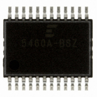
CS5460A-BSZ Cirrus Logic Inc, CS5460A-BSZ Datasheet - Page 47

CS5460A-BSZ
Manufacturer Part Number
CS5460A-BSZ
Description
IC ENERGY METERING 1PHASE 24SSOP
Manufacturer
Cirrus Logic Inc
Datasheet
1.CS5460A-BSZ.pdf
(54 pages)
Specifications of CS5460A-BSZ
Package / Case
24-SSOP
Input Impedance
30 KOhm
Measurement Error
0.1%
Voltage - I/o High
0.8V
Voltage - I/o Low
0.2V
Current - Supply
2.9mA
Voltage - Supply
4.75 V ~ 5.25 V
Operating Temperature
-40°C ~ 85°C
Mounting Type
Surface Mount
Meter Type
Single Phase
Output Voltage Range
2.4 V to 2.6 V
Output Current
1 uA
Input Voltage Range
2.4 V to 2.6 V
Input Current
25 nA
Power Dissipation
500 mW
Operating Temperature Range
- 40 C to + 85 C
Mounting Style
SMD/SMT
Ic Function
Single Phase Bi-directional Power / Energy IC
Brief Features
On-Chip Functions, AC Or DC System Calibration, Power Supply Monitor
Supply Voltage Range
3.3V To 5V
Rohs Compliant
Yes
Lead Free Status / RoHS Status
Lead free / RoHS Compliant
For Use With
CDB5460AU - EVALUATION BOARD FOR CS5460A
Lead Free Status / Rohs Status
Lead free / RoHS Compliant
Other names
598-1094-5
Available stocks
Company
Part Number
Manufacturer
Quantity
Price
Company:
Part Number:
CS5460A-BSZ
Manufacturer:
CIRRUS
Quantity:
2
Company:
Part Number:
CS5460A-BSZR
Manufacturer:
CIRRUS
Quantity:
8 000
Part Number:
CS5460A-BSZR
Manufacturer:
CIRRUS
Quantity:
20 000
5.5 Pulse-Rate Register
5.6 I,V,P,E Signed Output Register Results
5.7 I
5.8 Timebase Calibration Register
DS487F4
MSB
MSB
MSB
MSB
-(2
2
2
2
18
-1
0
0
Default** = 1.000
The Timebase Calibration Register is initialized to 1.0 on reset, allowing the device to function and perform com-
putations. The register can be loaded with the clock frequency error to compensate for a gain error caused by
the crystal/oscillator tolerance. The value is in the range 0.0 ≤ TBC < 2.0.
Address: 6
Default** = 32000.00Hz
The Pulse-Rate Register determines the frequency of the train of pulses output on the EOUT pin. Each EOUT
pulse represents a predetermined magnitude of real (billable) energy. The register’s smallest valid value is 2
but can be in 2
Address: 7 - 10
These signed registers contain the last value of the measured results of I, V, P, and E. The results are in the
range of -1.0 ≤ I, V, P, E < 1.0. The value is represented in two's complement notation, with the binary point
place to the right of the MSB (which is the sign bit). I, V, P, and E are output results registers which contain
signed values. Note that the I, V, and P Registers are updated every conversion cycle, while the E Register is
only updated after each computation cycle. The numeric format of this register is two’s complement notation.
Address: 11,12
These unsigned registers contain the last value of the calculated results of I
the range of 0.0 ≤ I
the left of the MSB. I
Address: 13
)
RMS
2
2
2
2
, V
17
-1
-2
-1
RMS
2
2
2
2
16
-2
-3
-2
Unsigned Output Register Results
-5
increments.
RMS
2
2
2
2
15
-3
-4
RMS
-3
,V
RMS
and V
2
2
2
2
14
-4
-5
-4
< 1.0. The value is represented in binary notation, with the binary point place to
RMS
2
2
2
2
13
-5
-6
-5
are output result registers which contain unsigned values.
2
2
2
2
12
-6
-7
-6
2
2
2
2
11
-7
-8
-7
.....
.....
.....
.....
2
2
2
2
-17
-18
-17
1
2
2
2
2
-18
-19
-18
0
RMS
2
2
2
2
-19
-20
-19
-1
and V
2
2
2
2
-20
-21
-20
-2
RMS
. The results are in
2
2
2
2
-21
-22
-21
-3
CS5460A
2
2
2
2
-22
-23
-22
-4
LSB
LSB
LSB
LSB
2
2
2
2
-23
-24
-23
-5
47
-4


