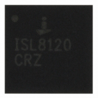
ISL8120CRZ Intersil, ISL8120CRZ Datasheet - Page 18

ISL8120CRZ
Manufacturer Part Number
ISL8120CRZ
Description
IC CTRLR PWM 2PHASE W/DVR 32-QFN
Manufacturer
Intersil
Datasheet
1.ISL8120IRZ.pdf
(35 pages)
Specifications of ISL8120CRZ
Pwm Type
Voltage Mode
Number Of Outputs
2
Frequency - Max
1.5MHz
Duty Cycle
90%
Voltage - Supply
3 V ~ 22 V
Buck
Yes
Boost
No
Flyback
No
Inverting
No
Doubler
No
Divider
No
Cuk
No
Isolated
No
Operating Temperature
0°C ~ 70°C
Package / Case
32-VQFN Exposed Pad, 32-HVQFN, 32-SQFN, 32-DHVQFN
Frequency-max
1.5MHz
Rohs Compliant
YES
Lead Free Status / RoHS Status
Lead free / RoHS Compliant
Available stocks
Company
Part Number
Manufacturer
Quantity
Price
Company:
Part Number:
ISL8120CRZ
Manufacturer:
Intersil
Quantity:
120
Part Number:
ISL8120CRZ
Manufacturer:
INTERSIL
Quantity:
20 000
Functional Pin Descriptions
GND (Pin 33)
The bottom pad is the signal and power ground plane. All
voltage levels are referenced to this pad. This pad provides a
return path for the low-side MOSFET drives and internal
power circuitries as well as all analog signals. Connect this
pad to the circuit ground with the shortest possible path
(more than 5 to 6 vias to the internal ground plane, placed on
the soldering pad are recommended).
VIN (Pin 16)
This pin is the input of the internal linear regulator. It should
be tied directly to the input rail. When used with an external
5V supply, this pin should be tied directly to PVCC. The
internal linear device is protected against reverse bias
generated by the remaining charge of the decoupling
capacitor at PVCC when losing the input rail.
VCC (Pin 26)
This pin provides bias power for the analog circuitry. An RC
filter is recommended between the connection of this pin to a
3V to 5.6V bias (typically PVCC). R is suggested to be a 5Ω
resistor. And in 3.3V applications, the R could be shorted to
allow the low end input in concerns of the VCC falling
threshold. The VCC decoupling capacitor C is strongly
recommended to be as large as a 10µF ceramic capacitor.
This pin can be powered either by the internal linear
regulator or by an external voltage source.
BOOT1, 2 (Pins 25, 17)
This pin provides the bootstrap bias for the high-side driver.
Internal bootstrap diodes connected to the PVCC pin provide
the necessary bootstrap charge. Its typical operational
voltage range is 2.5V to 5.6V.
UGATE1, UGATE2 (Pin 24, 18)
These pins provide the drive for the high-side devices and
should be connected to the MOSFETs’ gates.
PHASE1, PHASE2 (Pins 23,19)
Connect these pins to the source of the high-side MOSFETs
and the drain of the low-side MOSFETs. These pins
represent the return path for the high-side gate drives.
PVCC (Pin 21)
This pin is the output of the internal series linear regulator. It
provides the bias for both low-side and high-side drives. Its
operational voltage range is 3V to 5.6V. The decoupling
ceramic capacitor in the PVCC pin is 10µF.
LGATE1, LGATE2 (Pins 22, 20)
These pins provide the drive for the low-side devices and
should be connected to the MOSFETs’ gates.
FSYNC (Pin 5)
The oscillator switching frequency is adjusted by placing a
resistor (R
FS
) from this pin to GND. The internal oscillator
18
ISL8120
will lock to an external frequency source if this pin is
connected to a switching square pulse waveform, typically
the CLKOUT input signal from another ISL8120 or an
external clock. The internal oscillator synchronizes with the
leading edge of the input signal.
EN/FF1, EN/FF2 (Pins 4, 6)
These pins have triple functions. The voltage on EN/FF_ pin
is compared with a precision 0.8V threshold for system
enable to initiate soft-start. With a voltage lower than the
threshold, the corresponding channel can be disabled
independently. By connecting these pins to the input rail
through a voltage resistor divider, the input voltage can be
monitored for UVLO (undervoltage lockout ) function. The
undervoltage lockout and its hysteresis levels can be
programmed by these resistor dividers. The voltages on
these pins are also fed into the controller to adjust the
sawtooth amplitude of each channel independently to realize
the feed-forward function.
Furthermore, during fault (such as overvoltage, overcurrent,
and over-temperature) conditions, these pins (EN/FF_) are
pulled low to communicate the information to other cascaded
ICs.
PGOOD (Pin 8)
Provides an open drain Power-Good signal when both
channels are within 9% of the nominal output regulation
point with 4% hysteresis (13%/9%) and soft-start complete.
PGOOD monitors the outputs (VMON1/2) of the internal
differential amplifiers.
ISEN1A, ISEN2A (Pins 27, 15)
These pins are the non-inverting (+) inputs of the current
sensing amplifiers to provide r
resistor current sensing together with the ISEN1B, ISEN2B
pins.
ISEN1B, ISEN2B (Pins 28, 14)
These pins are the inverting (-) inputs of the current sensing
amplifiers to provide rDS(ON), DCR, or precision resistor
current sensing together with the ISEN1A, ISEN2A pins.
Refer to “Typical Application III (2-Phase Operation with
r
r
Operation with DCR Sensing)” on page 9 for DCR sensing
set up.
ISET (Pin 2)
This pin sources a 15µA offset current plus the average current
of both channels in multiphase mode or only Channel 1’s
current in independent mode. The voltage (V
external resistor (R
the local active channel(s).
ISHARE (Pin 3)
This pin is used for current sharing purposes and is
configured to current share bus representing all modules’
DS(ON)
DS(ON)
Sensing and Voltage Trimming)” on page 7 for
sensing set up and “Typical Application V (4 Phase
ISET
) represents the average current level of
DS(ON)
, DCR, or precision
ISET
) set by an
March 20, 2009
FN6641.0


