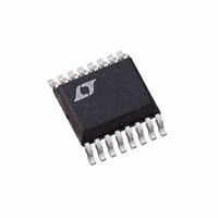
LTC3703EGN Linear Technology, LTC3703EGN Datasheet - Page 22

LTC3703EGN
Manufacturer Part Number
LTC3703EGN
Description
IC BUCK/BOOST SYNC ADJ 5A 16SSOP
Manufacturer
Linear Technology
Type
Step-Down (Buck), Step-Up (Boost)r
Datasheet
1.LTC3703EGNPBF.pdf
(32 pages)
Specifications of LTC3703EGN
Internal Switch(s)
No
Synchronous Rectifier
Yes
Number Of Outputs
1
Voltage - Output
0.8 ~ 93 V
Current - Output
5A
Frequency - Switching
100kHz ~ 600kHz
Voltage - Input
9.3 ~ 100 V
Operating Temperature
-40°C ~ 85°C
Mounting Type
Surface Mount
Package / Case
16-SSOP
Lead Free Status / RoHS Status
Contains lead / RoHS non-compliant
Power - Output
-
Available stocks
Company
Part Number
Manufacturer
Quantity
Price
Company:
Part Number:
LTC3703EGN
Manufacturer:
LINEAR
Quantity:
4
Part Number:
LTC3703EGN
Manufacturer:
LTNEAR
Quantity:
20 000
Company:
Part Number:
LTC3703EGN#PBF
Manufacturer:
LT
Quantity:
3 291
Part Number:
LTC3703EGN#PBF
Manufacturer:
LINEAR/凌特
Quantity:
20 000
Company:
Part Number:
LTC3703EGN#TRPBF
Manufacturer:
LT
Quantity:
3 291
Part Number:
LTC3703EGN#TRPBF
Manufacturer:
LTNEAR
Quantity:
20 000
Company:
Part Number:
LTC3703EGN-5
Manufacturer:
LT
Quantity:
10 000
Part Number:
LTC3703EGN-5
Manufacturer:
LINEAR/凌特
Quantity:
20 000
Company:
Part Number:
LTC3703EGN-5#PBF
Manufacturer:
LT
Quantity:
320
Part Number:
LTC3703EGN-5#PBF
Manufacturer:
LINEAR/凌特
Quantity:
20 000
APPLICATIONS INFORMATION
LTC3703
similar. However, note that the power dissipation equations
for the MOSFETs at maximum output current in a boost
converter are:
Boost Converter: Output Capacitor Selection
In boost mode, the output capacitor requirements are
more demanding due to the fact that the current waveform
is pulsed instead of continuous as in a buck converter.
The choice of component(s) is driven by the acceptable
ripple voltage which is affected by the ESR, ESL and bulk
capacitance as shown in Figure 15. The total output ripple
voltage is:
where the fi rst term is due to the bulk capacitance and
second term due to the ESR.
The choice of output capacitor is driven also by the RMS
ripple current requirement. The RMS ripple current is:
22
Figure 15. Output Voltage Ripple Waveform for a Boost Converter
P
P
I
Δ
RMS COUT
MAIN
SYNC
V
OUT
(
V
(AC)
OUT
=
=
=
D
–
⎡
⎢
⎢
⎣
2
I
1
MAX
O MAX
)
⎛
⎝ ⎜
V
(
V
≈
CC
1
O O UT
I
–
O MAX
⎛
⎝ ⎜
–
D
(
)
1
1
2
1
MAX
V
⎛
⎝ ⎜
–
V
⎛
⎝ ⎜
I
T
ESR
MAX
f C
D
1
H H IL
•
)
MAX
( )
–
•
I
⎞ ⎞
⎠ ⎟
MAX
1
D
OUT
(
V
I
MAX
MAX
COUT
+
V
⎞
⎠ ⎟
O
V
2
+
V
TH IL
–
(
⎞
⎠ ⎟
)
IN MIN
1
1
1
2
V
(
( )
+
(
–
R
(
IN MIN
ESR
RINGING DUE TO
TOTAL INDUCTANCE
(BOARD + CAP)
1 δ
δ
D
DR
(
+
)
⎤
⎥
⎥
⎦
MAX
)
R
( )
)(
f
DS ON
)
)
C
R
⎞
⎠ ⎟
(
MILLER
DS ON
(
)
+
)
)
•
At lower output voltages (less than 30V), it may be pos-
sible to satisfy both the output ripple voltage and RMS
ripple current requirements with one or more capacitors
of a single capacitor type. However, at output voltages
above 30V where capacitors with both low ESR and high
bulk capacitance are hard to fi nd, the best approach is to
use a combination of aluminum and ceramic capacitors
(see discussion in Input Capacitor section for the buck
converter). With this combination, the ripple voltage can
be improved signifi cantly. The low ESR ceremic capaci-
tor will minimize the ESR step, while the electrolytic will
supply the required bulk capacitance.
Boost Converter: Input Capacitor Selection
The input capacitor of a boost converter is less critical than
the output capacitor, due to the fact that the inductor is in
series with the input and the input current waveform is con-
tinuous. The input voltage source impedance determines
the size of the input capacitor, which is typically in the range
of 10μF to 100μF . A low ESR capacitor is recommended
though not as critical as for the output capacitor.
The RMS input capacitor ripple current for a boost con-
verter is:
Please note that the input capacitor can see a very high
surge current when a battery is suddenly connected to
the input of the converter and solid tantalum capacitors
can fail catastrophically under these conditions. Be sure
to specify surge-tested capacitors!
Boost Converter: Current Limit Programming
The LTC3703 provides current limiting in boost mode by
monitoring the V
comparing it to the voltage at I
calculate the expected voltage drop across the MOSFET
at the maximum desired inductor current and maximum
junction temperature. The maximum inductor current is
a function of both duty cycle and maximum load current,
so the limit must be set for the maximum expected duty
I
RMS CIN
(
)
= 0 3
. •
DS
of the main switch during its on-time and
V
IN MIN
L f
(
•
)
•
D
MAX
MAX
. To set the current limit,
3703fb


