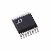
LTC3703EGN Linear Technology, LTC3703EGN Datasheet - Page 25

LTC3703EGN
Manufacturer Part Number
LTC3703EGN
Description
IC BUCK/BOOST SYNC ADJ 5A 16SSOP
Manufacturer
Linear Technology
Type
Step-Down (Buck), Step-Up (Boost)r
Datasheet
1.LTC3703EGNPBF.pdf
(32 pages)
Specifications of LTC3703EGN
Internal Switch(s)
No
Synchronous Rectifier
Yes
Number Of Outputs
1
Voltage - Output
0.8 ~ 93 V
Current - Output
5A
Frequency - Switching
100kHz ~ 600kHz
Voltage - Input
9.3 ~ 100 V
Operating Temperature
-40°C ~ 85°C
Mounting Type
Surface Mount
Package / Case
16-SSOP
Lead Free Status / RoHS Status
Contains lead / RoHS non-compliant
Power - Output
-
Available stocks
Company
Part Number
Manufacturer
Quantity
Price
Company:
Part Number:
LTC3703EGN
Manufacturer:
LINEAR
Quantity:
4
Part Number:
LTC3703EGN
Manufacturer:
LTNEAR
Quantity:
20 000
Company:
Part Number:
LTC3703EGN#PBF
Manufacturer:
LT
Quantity:
3 291
Part Number:
LTC3703EGN#PBF
Manufacturer:
LINEAR/凌特
Quantity:
20 000
Company:
Part Number:
LTC3703EGN#TRPBF
Manufacturer:
LT
Quantity:
3 291
Part Number:
LTC3703EGN#TRPBF
Manufacturer:
LTNEAR
Quantity:
20 000
Company:
Part Number:
LTC3703EGN-5
Manufacturer:
LT
Quantity:
10 000
Part Number:
LTC3703EGN-5
Manufacturer:
LINEAR/凌特
Quantity:
20 000
Company:
Part Number:
LTC3703EGN-5#PBF
Manufacturer:
LT
Quantity:
320
Part Number:
LTC3703EGN-5#PBF
Manufacturer:
LINEAR/凌特
Quantity:
20 000
APPLICATIONS INFORMATION
MODE/SYNC Pin (External Synchronization)
The internal LTC3703 oscillator can be synchronized
to an external oscillator by applying and clocking the
MODE/SYNC pin with a signal above 2V
oscillator locks to the external clock after the second clock
transition is received. When external synchronization is
detected, LTC3703 will operate in forced continuous mode.
If an external clock transition is not detected for three
successive periods, the internal oscillator will revert to the
frequency programmed by the R
oscillator can synchronize to frequencies between 100kHz
and 600kHz, independent of the frequency programmed by
the R
resistor be chosen such that the frequency programmed
by the R
the external clock. In this way, the best converter operation
(ripple, component stress, etc) is achieved if the external
clock signal is lost.
Fault Conditions: Output Overvoltage Protection
(Crowbar)
The output overvoltage crowbar is designed to blow a
system fuse in the input lead when the output of the regula-
tor rises much higher than nominal levels. This condition
causes huge currents to fl ow, much greater than in normal
operation. This feature is designed to protect against a
shorted top MOSFET; it does not protect against a failure
of the controller itself.
The comparator (MAX in the Functional Diagram) detects
overvoltage faults greater than 5% above the nominal
output voltage. When this condition is sensed the top
MOSFET is turned off and the bottom MOSFET is forced
on. The bottom MOSFET remains on continuously for as
long as the 0V condition persists; if V
level, normal operation automatically resumes.
Minimum On-Time Considerations (Buck Mode)
Minimum on-time t
that the LTC3703 is capable of turning the top MOSFET on
and off again. It is determined by internal timing delays
and the amount of gate charge required to turn on the
top MOSFET. Low duty cycle applications may approach
SET
SET
resistor. However, it is recommended that an R
resistor is close to the expected frequency of
ON(MIN)
is the smallest amount of time
SET
resistor. The internal
OUT
P-P
returns to a safe
. The internal
SET
this minimum on-time limit and care should be taken to
ensure that:
where t
If the duty cycle falls below what can be accommodated
by the minimum on-time, the LTC3703 will begin to skip
cycles. The output will be regulated, but the ripple current
and ripple voltage will increase. If lower frequency opera-
tion is acceptable, the on-time can be increased above
t
Pin Clearance/Creepage Considerations
The LTC3703 is available in two packages (GN16 and G28)
both with identical functionality. The GN16 package gives
the smallest size solution, however the 0.013" (minimum)
space between pins may not provide suffi cient PC board
trace clearance between high and low voltage pins in
higher voltage applications. Where clearance is an issue,
the G28 package should be used. The G28 package has
four unconnected pins between the all adjacent high volt-
age and low voltage pins, providing 5(0.0106") = 0.053"
clearance which will be suffi cient for most applications
up to 100V. For more information, refer to the printed
circuit board design standards described in IPC-2221
(www.ipc.org).
Effi ciency Considerations
The effi ciency of a switching regulator is equal to the out-
put power divided by the input power (x100%). Percent
effi ciency can be expressed as:
where L1, L2, etc. are the individual losses as a percentage
of input power. It is often useful to analyze the individual
losses to determine what is limiting the effi ciency and
what change would produce the most improvement.
Although all dissipative elements in the circuit produce
losses, four main sources usually account for most of the
losses in LTC3703 circuits: 1) LTC3703 V
MOSFET gate current, 3) I
transition losses.
ON(MIN)
%Effi ciency = 100% – (L1 + L2 + L3 + ...)
t
ON
=
ON(MIN)
for the same step-down ratio.
V
V
IN
OUT
•
f
is typically 200ns.
>
t
ON MIN
(
)
2
R losses, 4) Topside MOSFET
LTC3703
CC
current, 2)
25
3703fb


