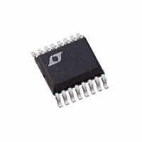
LTC3703EGN Linear Technology, LTC3703EGN Datasheet - Page 24

LTC3703EGN
Manufacturer Part Number
LTC3703EGN
Description
IC BUCK/BOOST SYNC ADJ 5A 16SSOP
Manufacturer
Linear Technology
Type
Step-Down (Buck), Step-Up (Boost)r
Datasheet
1.LTC3703EGNPBF.pdf
(32 pages)
Specifications of LTC3703EGN
Internal Switch(s)
No
Synchronous Rectifier
Yes
Number Of Outputs
1
Voltage - Output
0.8 ~ 93 V
Current - Output
5A
Frequency - Switching
100kHz ~ 600kHz
Voltage - Input
9.3 ~ 100 V
Operating Temperature
-40°C ~ 85°C
Mounting Type
Surface Mount
Package / Case
16-SSOP
Lead Free Status / RoHS Status
Contains lead / RoHS non-compliant
Power - Output
-
Available stocks
Company
Part Number
Manufacturer
Quantity
Price
Company:
Part Number:
LTC3703EGN
Manufacturer:
LINEAR
Quantity:
4
Part Number:
LTC3703EGN
Manufacturer:
LTNEAR
Quantity:
20 000
Company:
Part Number:
LTC3703EGN#PBF
Manufacturer:
LT
Quantity:
3 291
Part Number:
LTC3703EGN#PBF
Manufacturer:
LINEAR/凌特
Quantity:
20 000
Company:
Part Number:
LTC3703EGN#TRPBF
Manufacturer:
LT
Quantity:
3 291
Part Number:
LTC3703EGN#TRPBF
Manufacturer:
LTNEAR
Quantity:
20 000
Company:
Part Number:
LTC3703EGN-5
Manufacturer:
LT
Quantity:
10 000
Part Number:
LTC3703EGN-5
Manufacturer:
LINEAR/凌特
Quantity:
20 000
Company:
Part Number:
LTC3703EGN-5#PBF
Manufacturer:
LT
Quantity:
320
Part Number:
LTC3703EGN-5#PBF
Manufacturer:
LINEAR/凌特
Quantity:
20 000
APPLICATIONS INFORMATION
LTC3703
charge up the soft-start capacitor C
on RUN/SS reaches 0.9V, the LTC3703 begins operating
at its minimum on-time. As the RUN/SS voltage increases
from 1.4V to 3V, the duty cycle is allowed to increase
from 0% to 100%. The duty cycle control minimizes
input supply inrush current and elimates output voltage
overshoot at start-up and ensures current limit protection
even with a hard short. The RUN/SS voltage is internally
clamped at 4V.
If RUN/SS starts at 0V, the delay before starting is
approximately:
plus an additional delay, before the output will reach its
regulated value, of:
The start delay can be reduced by using diode D1 in
Figure 18.
MODE/SYNC Pin (Operating Mode and Secondary
Winding Control)
The MODE/SYNC pin is a dual function pin that can be used
for enabling or disabling pulse-skip mode operation and
also as an external clock input for synchronizing the internal
oscillator (see next section). Pulse-skip mode is enabled
when the MODE/SYNC pin is above 0.8V and is disabled,
i.e., forced continuous, when the pin is below 0.8V.
In addition to providing a logic input to force continuous
operation and external synchronization, the MODE/SYNC
pin provides a means to regulate a fl yback winding output
as shown in Figure 10c. The auxiliary output is taken from
a second winding on the core of the inductor, converting
it to a transformer. The auxiliary output voltage is set by
24
t
t
DELAY START
DELAY REG
OR 5V
3.3V
,
,
Figure 18. RUN/SS Pin Interfacing
≥
D1
3
=
V
4
4
1
μA
–
RUN/SS
μA
V
1
V
C
C
C
SS
SS
SS
=
=
( .
0 25
( . / )
0 5
s μF C
s μF C
SS
/ )
. When the voltage
SS
SS
RUN/SS
3703 F18
C
SS
the main output voltage and the turns ratio of the extra
winding to the primary winding as follows:
Since the secondary winding only draws current when the
synchronous switch is on, load regulation at the auxiliary
output will be relatively good as long as the main output
is running in continuous mode. As the load on the primary
output drops and the LTC3703 switches to pulse-skip mode
operation, the auxiliary output may not be able to maintain
regulation, especially if the load on the auxiliary output
remains heavy. To avoid this, the auxiliary output voltage
can be divided down with a conventional feedback resistor
string with the divided auxiliary output voltage fed back to
the MODE/SYNC pin. The MODE/SYNC threshold is trimmed
to 800mV with 20mV of hysteresis, allowing precise control
of the auxiliary voltage and is set as follows:
where R1 and R2 are shown in Figure 10c.
If the LTC3703 is operating in pulse-skip mode and the
auxiliary output voltage drops below V
SYNC pin will trip and the LTC3703 will resume continu-
ous operation regardless of the load on the main output.
Thus, the MODE/SYNC pin removes the requirement that
power must be drawn from the inductor primary in order
to extract power from the auxiliary winding. With the loop
in continuous mode (MODE/SYNC < 0.8V), the auxiliary
outputs may nominally be loaded without regard to the
primary output load.
The following table summarizes the possible states avail-
able on the MODE/SYNC pin:
Table 1
MODE/SYNC PIN
DC Voltage: 0V to 0.75V
DC Voltage: ≥ 0.87V
Feedback Resistors
Ext. Clock: 0V to ≥ 2V
V
V
SEC
SEC MIN
(
≈ (N + 1)V
)
≈
0 8
.
OUT
V
⎛
⎝ ⎜
1
+
R
R
2
1
⎞
⎠ ⎟
CONDITION
Forced Continuous
Current Reversal Enabled
Pulse-Skip Mode Operation
No Current Reversal
Regulating a Secondary Winding
Forced Continuous
Current Reversal Enabled
SEC(MIN)
, the MODE/
3703fb


