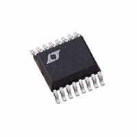
LTC3703EGN Linear Technology, LTC3703EGN Datasheet - Page 9

LTC3703EGN
Manufacturer Part Number
LTC3703EGN
Description
IC BUCK/BOOST SYNC ADJ 5A 16SSOP
Manufacturer
Linear Technology
Type
Step-Down (Buck), Step-Up (Boost)r
Datasheet
1.LTC3703EGNPBF.pdf
(32 pages)
Specifications of LTC3703EGN
Internal Switch(s)
No
Synchronous Rectifier
Yes
Number Of Outputs
1
Voltage - Output
0.8 ~ 93 V
Current - Output
5A
Frequency - Switching
100kHz ~ 600kHz
Voltage - Input
9.3 ~ 100 V
Operating Temperature
-40°C ~ 85°C
Mounting Type
Surface Mount
Package / Case
16-SSOP
Lead Free Status / RoHS Status
Contains lead / RoHS non-compliant
Power - Output
-
Available stocks
Company
Part Number
Manufacturer
Quantity
Price
Company:
Part Number:
LTC3703EGN
Manufacturer:
LINEAR
Quantity:
4
Part Number:
LTC3703EGN
Manufacturer:
LTNEAR
Quantity:
20 000
Company:
Part Number:
LTC3703EGN#PBF
Manufacturer:
LT
Quantity:
3 291
Part Number:
LTC3703EGN#PBF
Manufacturer:
LINEAR/凌特
Quantity:
20 000
Company:
Part Number:
LTC3703EGN#TRPBF
Manufacturer:
LT
Quantity:
3 291
Part Number:
LTC3703EGN#TRPBF
Manufacturer:
LTNEAR
Quantity:
20 000
Company:
Part Number:
LTC3703EGN-5
Manufacturer:
LT
Quantity:
10 000
Part Number:
LTC3703EGN-5
Manufacturer:
LINEAR/凌特
Quantity:
20 000
Company:
Part Number:
LTC3703EGN-5#PBF
Manufacturer:
LT
Quantity:
320
Part Number:
LTC3703EGN-5#PBF
Manufacturer:
LINEAR/凌特
Quantity:
20 000
OPERATION
drop in the feedback voltage relative to the reference. The
COMP voltage then rises, increasing the duty ratio until
the output feedback voltage again matches the reference
voltage. In normal operation, the top MOSFET is turned
on when the RS latch is set by the on-chip oscillator and
is turned off when the PWM comparator trips and resets
the latch. The PWM comparator trips at the proper duty
ratio by comparing the error amplifi er output (after being
“compensated” by the line feedforward multiplier) to a
sawtooth waveform generated by the oscillator. When the
top MOSFET is turned off, the bottom MOSFET is turned
on until the next cycle begins or, if pulse-skip mode op-
eration is enabled, until the inductor current reverses as
determined by the reverse current comparator. MAX and
MIN comparators ensure that the output never exceed
±5% of nominal value by monitoring V
output back into regulation quickly by either keeping the top
MOSFET off or forcing maximum duty cycle. The operation
of its other features—fast transient response, outstanding
line regulation, strong gate drivers, short-circuit protection
and shutdown/soft-start—are described below.
Fast Transient Response
The LTC3703 uses a fast 25MHz op amp as an error ampli-
fi er. This allows the compensation network to be optimized
for better load transient response. The high bandwidth of
the amplifi er, along with high switching frequencies and
low value inductors, allow very high loop crossover fre-
quencies. The 800mV internal reference allows regulated
output voltages as low as 800mV without external level
shifting amplifi ers.
Line Feedforward Compensation
The LTC3703 achieves outstanding line transient response
using a patented feedforward correction scheme. With
this circuit the duty cycle is adjusted instantaneously to
changes in input voltage, thereby avoiding unacceptable
overshoot or undershoot. It has the added advantage of
making the DC loop gain independent of input voltage.
Figure 2 shows how large transient steps at the input have
little effect on the output voltage.
(Refer to Functional Diagram)
FB
and forcing the
Strong Gate Drivers
The LTC3703 contains very low impedance drivers capable
of supplying amps of current to slew large MOSFET gates
quickly. This minimizes transition losses and allows paral-
leling MOSFETs for higher current applications. A 100V
fl oating high side driver drives the topside MOSFET and
a low side driver drives the bottom side MOSFET (see
Figure 3). They can be powered from either a separate
DC supply or a voltage derived from the input or output
voltage (see MOSFET Driver Supplies section). The bottom
side driver is supplied directly from the DRV
top MOSFET drivers are biased from fl oating bootstrap
capacitor, C
cycle through an external diode from DRV
MOSFET turns off. In pulse-skip mode operation, where
it is possible that the bottom MOSFET will be off for an
extended period of time, an internal counter guarantees
that the bottom MOSFET is turned on at least once every
10 cycles for 10% of the period to refresh the bootstrap
capacitor. An undervoltage lockout keeps the LTC3703
shut down unless this voltage is above 8.7V.
The bottom driver has an additional feature that helps
minimize the possibility of external MOSFET shoot-through.
When the top MOSFET turns on, the switch node dV/dt
pulls up the bottom MOSFET’s internal gate through the
Miller capacitance, even when the bottom driver is holding
the gate terminal at ground. If the gate is pulled up high
enough, shoot-through between the topside and bottom
50mV/DIV
20V/DIV
2A/DIV
V
OUT
V
IN
I
L
V
I
25V TO 60V V
LOAD
OUT
B
Figure 2. Line Transient Performance
, which normally is recharged during each off
= 12V
= 1A
IN
STEP
20μs/DIV
LTC3703
CC
3703 F02
when the top
CC
pin. The
3703fb
9


