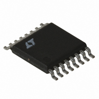
LT3433IFE Linear Technology, LT3433IFE Datasheet - Page 11

LT3433IFE
Manufacturer Part Number
LT3433IFE
Description
IC CONV DC/DC 200KHZ SW 16-TSSOP
Manufacturer
Linear Technology
Type
Step-Down (Buck), Step-Up (Boost)r
Datasheet
1.LT3433EFEPBF.pdf
(16 pages)
Specifications of LT3433IFE
Internal Switch(s)
Yes
Synchronous Rectifier
No
Number Of Outputs
1
Voltage - Output
3.3 ~ 20 V
Current - Output
500mA
Frequency - Switching
200kHz
Voltage - Input
4 ~ 60 V
Operating Temperature
-40°C ~ 125°C
Mounting Type
Surface Mount
Package / Case
16-TSSOP Exposed Pad, 16-eTSSOP, 16-HTSSOP
Lead Free Status / RoHS Status
Contains lead / RoHS non-compliant
Power - Output
-
Available stocks
Company
Part Number
Manufacturer
Quantity
Price
Part Number:
LT3433IFE
Manufacturer:
LINEAR/凌特
Quantity:
20 000
Company:
Part Number:
LT3433IFE#PBF
Manufacturer:
LT
Quantity:
5 000
Part Number:
LT3433IFE#PBF
Manufacturer:
LINEAR/凌特
Quantity:
20 000
Part Number:
LT3433IFE#TRPBF
Manufacturer:
LT凌特厂
Quantity:
20 000
APPLICATIO S I FOR ATIO
Operational duty cycle is a function of voltage imposed
across the switched inductance and switch on/off times.
Using the relation for change in current in an inductor:
and putting the application variables into the above rela-
tion yields:
Current conservation in an inductor dictates I
so plugging in the above relations and solving for DC yields:
In order to solve the above equations, inductor ripple
current ( I) must be determined so I
As I is a function of DC and vice-versa, the solution is
iterative. Seed I and solve for DC. Using the resulting
value for DC, solve for I. Use the resulting I as the new
seed value and repeat. The calculated value for DC can be
used once the resulting I is close (<1%) to the seed value.
I follows the relation:
R
(in A/A)
V
V
I
I
I
R
+ R
• (R
• (R
DC
[V
V
DC
[V
VIN
IN
BIAS
I = V • t/L
I
I
I
F1
F2
F1
L
BST
OUT
CESR
I = (V
ON(BRIDGED)
ON(BUCK)
OFF
IN
IN
(BRIDGED)
(BUCK)
= Inductor series resistance
= V
L
+ V
SWH
L
= Switch node catch diode forward voltage
= Pass diode forward voltage
= V
)]
– I
– I
= Boosted switch drive currents I
= V
+ R
= [(1 – DC)/f
= Grounded switch drive currents I
IN
= Output capacitor ESR
OUT
F2
SW
SW
IN
+ R
BIAS
switched current
ESR
= [V
]
quiescent input current
• (R
• (R
= (DC/f
+ V
L
)]
= [V
quiescent input current
+ R
OUT
= (DC/f
SWH
F1
SWH
U
ESR
OUT
+ V
+ V
O
O
+ R
+ 2R
• L)[V
• L][V
)]
F2
+ V
F1
O
SWL
U
– I
• L)[V
+ V
L
F1
+ 2R
SW
IN
OUT
+ V
F2
+ 2R
– V
IN
• R
– I
F2
+ V
ESR
– I
OUT
L
SW
W
L
– I
SW
)(1 – DC)/(L • f
+ R
F1
) + V
SW
SW
• (R
– V
+ V
can be calculated.
ESR
VBST
• (R
• (R
F1
F2
L
F2
) + V
]
+ R
SWH
/I
– I
– I
L
SW
ON
U
+ R
SW
ESR
SW
VOUT
OUT
+ R
(in A/A)
= I
ESR
)]/
O
+
SWL
/I
)
OFF
SW
)]/
,
PowerPath is a trademark of Linear Technology Corporation
Once DC is determined, maximum output current can be
determined using current conservation on the converter
output:
P
corresponding to the power loss in the converter. P
quiescent power dissipated by the LT3433. P
loss associated with the power path during the switch on
interval, and P
with the switch off interval.
P
Efficiency (E) is described as P
Efficiency = {1 + (P
Empirical determination of converter capabilities is ac-
complished by monitoring inductor currents with a cur-
rent probe under various input voltages and load currents.
Decreasing input voltage or increasing load current re-
sults in an inductor current increase. When peak inductor
currents reach the switch current limit value, maximum
output current is achieved. Limiting the inductor currents
to the LT3433 specified W/C current limit of 0.5V (cold)
will allow margin for operating limit variations. These
limitations should be evaluated at the operating tempera-
ture extremes required by the application to assure robust
performance.
IN
LOSS
Bridged Operation: I
Buck Operation:
P
P
P
+ I
P
V
I
P
R
OUT
= P
VIN
BIAS
SWON(BRIDGED)
SWON(BUCK)
OUT
SWOFF
CESR
SW
equals the sum of the power loss terms:
OUT
)
= V
2
•
• V
= V
]
• (I
= (1 – DC) • [I
+ P
IN
BST
OUT
OUT
SW
• I
LOSS
SWOFF
+ R
• (
VIN
– I
= DC • [I
• I
VIN
, where P
BIAS
CESR
BIAS
= DC • [I
BST
is the PowerPath
+ P
(1 +
I
– I
– I
+
OUT(MAX)
OUT(MAX)
• (I
SW
SW
BIAS
BIAS
OUT
SW
OUT
LOSS
SW
2
• (V
BST
)
+ P
• (R
• (1 –
2
) + R
OUT
2
]
F1
= P
• (R
SWON
= I
+
= I
SWH
+ V
/P
CESR
SW
SW
SWON
OUT
SWH
IN
BST
F2
+ R
+ P
TM
, so:
• [1 – DC •
• (1 – DC •
) + I
)] – I
• I
) – I
loss associated
+ R
+ P
SWOFF
L
OUT
) + I
LT3433
SW
SWOFF
SWL
BIAS
SWON
BIAS
2
SW
2
]
)/P
• R
+ R
11
IC
–
•
OUT
+ P
is the
L
is the
BST
L
+
)
3433f
}
IC
–1
)
,


