LT3433IFE Linear Technology, LT3433IFE Datasheet - Page 6

LT3433IFE
Manufacturer Part Number
LT3433IFE
Description
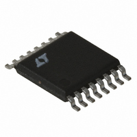
IC CONV DC/DC 200KHZ SW 16-TSSOP
Manufacturer
Linear Technology
Type
Step-Down (Buck), Step-Up (Boost)r
Datasheet
1.LT3433EFEPBF.pdf
(16 pages)
Specifications of LT3433IFE
Internal Switch(s)
Yes
Synchronous Rectifier
No
Number Of Outputs
1
Voltage - Output
3.3 ~ 20 V
Current - Output
500mA
Frequency - Switching
200kHz
Voltage - Input
4 ~ 60 V
Operating Temperature
-40°C ~ 125°C
Mounting Type
Surface Mount
Package / Case
16-TSSOP Exposed Pad, 16-eTSSOP, 16-HTSSOP
Lead Free Status / RoHS Status
Contains lead / RoHS non-compliant
Power - Output
-
Available stocks
Company
Part Number
Manufacturer
Quantity
Price
Part Number:
LT3433IFE
Manufacturer:
LINEAR/凌特
Quantity:
20 000
Company:
Part Number:
LT3433IFE#PBF
Manufacturer:
LT
Quantity:
5 000
Part Number:
LT3433IFE#PBF
Manufacturer:
LINEAR/凌特
Quantity:
20 000
Part Number:
LT3433IFE#TRPBF
Manufacturer:
LT凌特厂
Quantity:
20 000
LT3433
PI FU CTIO S
V
ing input of the error amplifier is connected to an internal
1.231V reference. The V
divider from the converter output. Values for the resistor
connected from V
nected from V
gram converter output voltage (V
relation:
The V
high value feedback resistors could cause a converter
output that is slightly higher than expected. Bias current
error at the output can be estimated as:
The voltage on V
frequency through a “frequency-foldback” function. When
the V
than the 200kHz typical operating frequency. The oscilla-
tor frequency slows with reduced voltage on the pin, down
to 50kHz when V
The V
through a “current-limit foldback” function. At V
maximum switch current is reduced to half of the normal
value. The current limit value increases linearly until V
reaches 0.6V when the normal maximum switch current
level is restored. The frequency and current-limit foldback
functions add robustness to short-circuit protection and
help prevent inductor current runaway during start-up.
SS (Pin 10): Soft Start. Connect a capacitor (C
pin to ground. The output voltage of the LT3433 error
amplifier corresponds to the peak current sense amplifier
output detected before resetting the switch output(s). The
soft-start circuit forces the error amplifier output to a zero
peak current for start-up. A 5 A current is forced from the
SS pin onto an external capacitor. As the SS pin voltage
ramps up, so does the LT3433 internally sensed peak cur-
rent limit. This forces the converter output current to ramp
from zero until normal output regulation is achieved. This
function reduces output overshoot on converter start-up.
6
FB
V
U
(Pin 7): Error Amplifier Inverting Input. The noninvert-
OUT
V
FB
FB
OUT(BIAS)
FB
pin voltage is below 0.8V, the oscillator runs slower
pin input bias current is 35nA, so use of extremely
= 1.231 • (R
pin voltage also controls switch current limit
U
FB
= 35nA • R
to ground (R
FB
FB
OUT
= 0V.
U
also controls the LT3433 oscillator
FB1
to V
+ R
FB
FB
FB1
pin is connected to a resistor
FB2
FB2
(R
)/R
FB1
) can be calculated to pro-
FB2
) and the resistor con-
OUT
) via the following
SS
FB
) from this
= 0V, the
FB
The time from V
be calculated given a capacitor C
SHDN (Pin 11): Shutdown. If the SHDN pin is externally
pulled below 0.5V, low current shutdown mode is initiated.
During shutdown mode, all internal functions are disabled,
and I
a digital input, however, there is a small amount of input
hysteresis built into the SHDN circuit to help assure glitch-
free mode switching. If shutdown is not desired, connect
the SHDN pin to V
V
circuitry is powered from this supply, which is internally
regulated to 2.5V through an on-board linear regulator.
Current drive for this regulator is sourced from the V
The V
The V
above the regulated voltage allows the use of external power
for much of the LT3433 circuitry. When using external drive,
this pin should be driven above 3V to assure the internal
supply is completely disabled. This pin is typically diode-
connected to the converter output to maximize conversion
efficiency. This pin must be bypassed with at least a 0.1 F
ceramic capacitor to SGND.
V
compared with the voltage on V
operation in single or 2-switch mode. When the ratios of
the two voltages are such that a >75% duty cycle is required
for regulation, the low side switch is enabled. Drive bias for
the low side switch is also derived directly from this pin.
PWRGND (Pin 14): High Current Ground Reference. This
is the current return for the low side switch and corresponds
to the emitter of the low side switch transistor.
SW_L (Pin 15): Ground Referenced Switch Output. This pin
is the collector of the low side switch transistor. The low
side switch shorts the SW_L pin to PWRGND when enabled.
The series impedance of the ground-referenced switch is
0.6 .
Exposed Pad (Pin 17): Exposed Pad must be soldered to
PCB ground for optimal thermal performance.
BIAS
OUT
t
SS
CC
BIAS
(Pin 13): Converter Output Pin. This pin voltage is
BIAS
(Pin 12): Internal Local Supply. Much of the LT3433
= (2.7 • 10
is reduced to 10 A. This pin is intended to receive
supply only sources current, so forcing this pin
supply is short-circuit protected to 5mA.
SS
5
)C
= 0V to maximum available current can
IN
.
SS
or 0.27s/ F
SS
IN
as:
internally to control
IN
pin.
3433f


