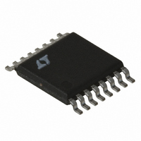
LT3433IFE Linear Technology, LT3433IFE Datasheet - Page 8

LT3433IFE
Manufacturer Part Number
LT3433IFE
Description
IC CONV DC/DC 200KHZ SW 16-TSSOP
Manufacturer
Linear Technology
Type
Step-Down (Buck), Step-Up (Boost)r
Datasheet
1.LT3433EFEPBF.pdf
(16 pages)
Specifications of LT3433IFE
Internal Switch(s)
Yes
Synchronous Rectifier
No
Number Of Outputs
1
Voltage - Output
3.3 ~ 20 V
Current - Output
500mA
Frequency - Switching
200kHz
Voltage - Input
4 ~ 60 V
Operating Temperature
-40°C ~ 125°C
Mounting Type
Surface Mount
Package / Case
16-TSSOP Exposed Pad, 16-eTSSOP, 16-HTSSOP
Lead Free Status / RoHS Status
Contains lead / RoHS non-compliant
Power - Output
-
Available stocks
Company
Part Number
Manufacturer
Quantity
Price
Part Number:
LT3433IFE
Manufacturer:
LINEAR/凌特
Quantity:
20 000
Company:
Part Number:
LT3433IFE#PBF
Manufacturer:
LT
Quantity:
5 000
Part Number:
LT3433IFE#PBF
Manufacturer:
LINEAR/凌特
Quantity:
20 000
Part Number:
LT3433IFE#TRPBF
Manufacturer:
LT凌特厂
Quantity:
20 000
APPLICATIO S I FOR ATIO
LT3433
Overview
The LT3433 is a high input voltage range, step-up/step-
down DC/DC converter IC using a 200kHz constant fre-
quency, current mode architecture. Dual internal switches
allow the full input voltage to be imposed across the
switched inductor, such that both step-up and step-down
modes of operation can be realized using the same single
inductor topology.
The LT3433 has provisions for high efficiency, low load
operation for battery-powered applications. Burst Mode
operation reduces average quiescent current to 100 A in
no load conditions. A low current shutdown mode can also
be activated, reducing total quiescent current to 10 A.
Much of the LT3433’s internal circuitry is biased from an
internal low voltage linear regulator. The output of this
regulator is brought out to the V
ing of the internal regulator. The associated internal
circuitry can be powered directly from the output of the
converter, increasing overall converter efficiency. Using
externally derived power also eliminates the IC’s power
dissipation associated with the internal V
regulator.
Theory of Operation (See Block Diagram)
The LT3433 senses converter output voltage via the V
pin. The difference between the voltage on this pin and an
internal 1.231V reference is amplified to generate an error
voltage on the V
for the current sense comparator.
During normal operation, the LT3433 internal oscillator
runs at 200kHz. At the beginning of each oscillator cycle,
the switch drive is enabled. The switch drive stays enabled
until the sensed switch current exceeds the V
threshold for the current sense comparator and, in turn,
disables the switch driver. If the current comparator
threshold is not obtained for the entire oscillator cycle, the
switch driver is disabled at the end of the cycle for 250ns.
This minimum off-time mode of operation assures regen-
eration of the V
If the converter input and output voltages are close
together, proper operation in normal buck configuration
would require high duty cycles. The LT3433 senses this
8
BST
C
pin which is, in turn, used as a threshold
U
bootstrapped supply.
U
BIAS
W
pin, allowing bypass-
IN
U
C
to V
-derived
BIAS
FB
condition as requiring a duty cycle greater than 75%. If
such a condition exists, a second switch is enabled during
the switch on time, which acts to pull the output side of the
inductor to ground. This “bridged” operation allows volt-
age conversion to continue when V
exceeds V
Shutdown
The LT3433 incorporates a low current shutdown mode
where all IC functions are disabled and the V
reduced to 10 A. Pulling the SHDN pin down to 0.4V or
less activates shutdown mode.
Burst Mode Operation
The LT3433 employs low current Burst Mode functionality
to maximize efficiency during no load and low load condi-
tions. Burst Mode function is disabled by shorting the
BURST_EN pin to either V
function is enabled by shorting BURST_EN to SGND.
In certain wide current range applications, the IC could
enter burst operation during normal load conditions. If the
additional output ripple and noise generated by Burst
Mode operation is not desired for normal operation,
BURST_EN can be biased using an external supply that is
disabled during a no-load condition. This enables Burst
Mode operation only when it is required. The BURST_EN
pin typically draws 35 A when Burst Mode operation is
disabled (V
75 A with V
When the required switch current, sensed via the V
voltage, is below 30% of maximum, the Burst Mode
function is employed. When the voltage on V
the 30% load level, that level of sense current is latched
into the IC. If the output load requires less than this latched
current level, the converter will overdrive the output slightly
during each switch cycle. This overdrive condition forces
the voltage on the V
voltage on V
is disabled, and the LT3433 shuts down most of its internal
circuitry, reducing quiescent current to 100 A. When the
voltage on the V
returns to normal operation and switching resumes.
IN
BURST_EN
.
BURST_EN
C
drops below the 15% load level, switching
C
pin climbs back to 20% load level, the IC
C
= 2V.
pin to continue to drop. When the
2V) and will draw no more than
BIAS
or V
OUT
OUT
approaches or
. Burst Mode
C
drops below
IN
current is
C
3433f
pin


