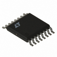
LT3433IFE Linear Technology, LT3433IFE Datasheet - Page 9

LT3433IFE
Manufacturer Part Number
LT3433IFE
Description
IC CONV DC/DC 200KHZ SW 16-TSSOP
Manufacturer
Linear Technology
Type
Step-Down (Buck), Step-Up (Boost)r
Datasheet
1.LT3433EFEPBF.pdf
(16 pages)
Specifications of LT3433IFE
Internal Switch(s)
Yes
Synchronous Rectifier
No
Number Of Outputs
1
Voltage - Output
3.3 ~ 20 V
Current - Output
500mA
Frequency - Switching
200kHz
Voltage - Input
4 ~ 60 V
Operating Temperature
-40°C ~ 125°C
Mounting Type
Surface Mount
Package / Case
16-TSSOP Exposed Pad, 16-eTSSOP, 16-HTSSOP
Lead Free Status / RoHS Status
Contains lead / RoHS non-compliant
Power - Output
-
Available stocks
Company
Part Number
Manufacturer
Quantity
Price
Part Number:
LT3433IFE
Manufacturer:
LINEAR/凌特
Quantity:
20 000
Company:
Part Number:
LT3433IFE#PBF
Manufacturer:
LT
Quantity:
5 000
Part Number:
LT3433IFE#PBF
Manufacturer:
LINEAR/凌特
Quantity:
20 000
Part Number:
LT3433IFE#TRPBF
Manufacturer:
LT凌特厂
Quantity:
20 000
APPLICATIO S I FOR ATIO
Antislope Compensation
Most current mode switching controllers use slope com-
pensation to prevent current mode instability. The LT3433
is no exception. A slope compensation circuit imposes an
artificial ramp on the sensed current to increase the rising
slope as duty cycle increases. Unfortunately, this addi-
tional ramp corrupts the sensed current value, reducing
the achievable current limit value by the same amount as
the added ramp represents. As such, current limit is
typically reduced as duty cycles increase.
The LT3433 contains circuitry to eliminate the current limit
reduction associated with slope-compensation, or anti-
slope compensation. As the slope compensation ramp is
added to the sensed current, a similar ramp is added to the
current limit threshold reference. The end result is that
current limit is not compromised so the LT3433 can
provide full power regardless of required duty cycle.
Mode Switching
The LT3433 switches between buck and buck/boost modes
of operation automatically. While in buck mode, if the
converter input voltage becomes close enough to the
output voltage to require a duty cycle greater than 75%,
the LT3433 enables a second switch which pulls the
output side of the inductor to ground during the switch-on
time. This “bridged” switching configuration allows volt-
age conversion to continue when V
than V
When the converter input voltage falls to where the duty
cycle required for continuous buck operation is greater
than 75%, the LT3433 enables its ground-referred switch,
changing the converter operation to a dual-switch bridged
configuration. Because the voltage available across the
switched inductor is greater while bridged, operational
duty cycle will decrease. Voltage drops associated with
external diodes and loss terms are estimated internally so
that required operating duty cycle can be calculated re-
gardless of specific operating voltages.
In the simplest terms, a buck DC/DC converter switches
the V
IN
OUT
side of the inductor, while a boost converter
.
U
U
IN
W
approaches or is less
U
switches the V
bridged topology merges the elements of buck and boost
topologies, providing switches on both sides of the induc-
tor. Operating both switches simultaneously achieves
both step-up and step-down functionality.
Maximum duty cycle capability (DC
capabilities of a buck converter. As V
the required duty cycle increases until DC
beyond which the converter loses regulation. With a
second switch bridging the switched inductor between V
and ground, the entire input voltage is imposed across the
inductor during the switch-on time, which subsequently
reduces the duty cycle required to maintain regulation.
Using this topology, regulation is maintained as V
proaches or drops below V
Inductor Selection
The primary criterion for inductor value selection in LT3433
applications is the ripple current created in that inductor.
Design considerations for ripple current are converter
output capabilities in bridged mode, output voltage ripple
and the ability of the internal slope compensation wave-
form to prevent current mode instability.
Step-Up/Step-Down (V
V
V
V
IN
IN
IN
OUT
Step-Down (V
SW
SW
C
C
C
Step-Up (V
IN
IN
IN
side of the inductor. The LT3433
D
D
OUT
IN
L
L
L
IN
IN
> V
< V
.
> V
OUT
OUT
SW
SW
OUT
MAX
D
D
or V
)
IN
)
) gates the dropout
– V
IN
3433 F01
V
V
V
C
C
C
< V
OUT
OUT
OUT
MAX
OUT
OUT
OUT
OUT
LT3433
OUT
is reduced,
is reached,
)
IN
9
3433f
ap-
IN


