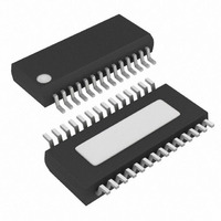
MAX1715EEI Maxim Integrated Products, MAX1715EEI Datasheet - Page 16

MAX1715EEI
Manufacturer Part Number
MAX1715EEI
Description
IC CTRLR DC DUAL STPDWN 28-QSOP
Manufacturer
Maxim Integrated Products
Type
Step-Down (Buck)r
Datasheet
1.MAX1715EEI.pdf
(25 pages)
Specifications of MAX1715EEI
Internal Switch(s)
No
Synchronous Rectifier
Yes
Number Of Outputs
2
Voltage - Output
1V, 1.8V, 2.5V, 3.3V, Adj
Current - Output
8A
Frequency - Switching
200kHz, 300kHz, 420kHz, 540kHz
Voltage - Input
2 ~ 28 V
Operating Temperature
-40°C ~ 85°C
Mounting Type
Surface Mount
Package / Case
28-QSOP
Power - Output
640mW
Output Voltage
1 V to 5.5 V, 3.3 V, 2.5 V
Output Current
8 A
Input Voltage
2 V to 28 V
Mounting Style
SMD/SMT
Maximum Operating Temperature
+ 85 C
Minimum Operating Temperature
- 40 C
Case
SSOP
Dc
05+
Lead Free Status / RoHS Status
Contains lead / RoHS non-compliant
Available stocks
Company
Part Number
Manufacturer
Quantity
Price
Part Number:
MAX1715EEI
Manufacturer:
MAXIM/美信
Quantity:
20 000
Company:
Part Number:
MAX1715EEI+
Manufacturer:
MAXIM
Quantity:
583
Part Number:
MAX1715EEI+
Manufacturer:
MAXIM/美信
Quantity:
20 000
Company:
Part Number:
MAX1715EEI+T
Manufacturer:
MAX
Quantity:
7 400
Part Number:
MAX1715EEI+T
Manufacturer:
MAXIM/美信
Quantity:
20 000
Part Number:
MAX1715EEI-T
Manufacturer:
MAXIM/美信
Quantity:
20 000
Company:
Part Number:
MAX1715EEI-TG069
Manufacturer:
MAXIN
Quantity:
2 268
Part Number:
MAX1715EEI-TG069
Manufacturer:
MAXOM
Quantity:
20 000
Ultra-High Efficiency, Dual Step-Down
Controller for Notebook Computers
16
Figure 6. Reducing the Switching-Node Rise Time
place the IC close to the low-side MOSFET with short,
direct traces, making a Kelvin sense connection to the
source and drain terminals.
The DH and DL drivers are optimized for driving mod-
erate-size, high-side and larger, low-side power
MOSFETs. This is consistent with the low duty factor
seen in the notebook CPU environment, where a large
V
circuit monitors the DL output and prevents the high-
side FET from turning on until DL is fully off. There must
be a low-resistance, low-inductance path from the DL
driver to the MOSFET gate for the adaptive dead-time
circuit to work properly. Otherwise, the sense circuitry
in the MAX1715 will interpret the MOSFET gate as “off”
while there is actually still charge left on the gate. Use
very short, wide traces measuring 10 to 20 squares (50
to 100 mils wide if the MOSFET is 1 inch from the
MAX1715).
The dead time at the other edge (DH turning off) is
determined by a fixed 35ns (typ) internal delay.
The internal pull-down transistor that drives DL low is
robust, with a 0.5Ω typical on-resistance. This helps
prevent DL from being pulled up during the fast rise-
time of the inductor node, due to capacitive coupling
from the drain to the gate of the low-side synchronous-
rectifier MOSFET. However, for high-current applica-
tions, you might still encounter some combinations of
high- and low-side FETs that will cause excessive gate-
drain coupling, which can lead to efficiency-killing,
EMI-producing shoot-through currents. This is often
remedied by adding a resistor in series with BST,
which increases the turn-on time of the high-side FET
without degrading the turn-off time (Figure 6).
BATT
______________________________________________________________________________________
MAX1715
- V
OUT
differential exists. An adaptive dead-time
MOSFET Gate Drivers (DH, DL)
BST
DH
LX
5Ω
+5V
V
IN
Power-on reset (POR) occurs when V
approximately 2V, resetting the fault latch and soft-start
counter and preparing the PWM for operation. V
undervoltage lockout (UVLO) circuitry inhibits switching
and forces the DL gate driver high (to enforce output
overvoltage protection) until V
whereupon an internal digital soft-start timer begins to
ramp up the maximum allowed current limit. The ramp
occurs in five steps: 20%, 40%, 60%, 80%, and 100%;
100% current is available after 1.7ms ±50%.
A continuously adjustable analog soft-start function can
be realized by adding a capacitor in parallel with the
ILIM external resistor. This soft-start method requires a
minimum interval between power-down and power-up
to discharge the capacitor.
The output voltage is continuously monitored for under-
voltage by the PGOOD comparator. In shutdown, soft-
start, and standby modes, PGOOD is actively held low.
After digital soft-start has terminated, PGOOD is
released if both the outputs are within 5.5% of the error
comparator threshold. The PGOOD output is a true
open-drain type with no parasitic ESD diodes. Note
that the PGOOD undervoltage detector is completely
independent of the output UVP fault detector.
The overvoltage protection circuit is designed to pro-
tect against a shorted high-side MOSFET by drawing
high current and blowing the battery fuse. The output
voltage is continuously monitored for overvoltage. If the
output is more than 10.5% above the trip level of the
error amplifier, OVP is triggered and the circuit shuts
down. The DL low-side gate-driver output is then
latched high until SHDN is toggled or V
cycled below 1V. This action turns on the synchronous-
rectifier MOSFET with 100% duty and, in turn, rapidly
discharges the output filter capacitor and forces the
output to ground. If the condition that caused the over-
voltage (such as a shorted high-side MOSFET) per-
sists, the battery fuse will blow. DL is also kept high
continuously when V
shutdown mode (Table 3).
Note that DL latching high causes the output voltage to
go slightly negative, due to energy stored in the output
LC at the instant OVP activates. If the load can’t toler-
ate being forced to a negative voltage, it may be desir-
able to place a power Schottky diode across the output
to act as a reverse-polarity clamp (Figure 1).
Output Overvoltage Protection (OVP)
Power-Good Output (PGOOD)
POR, UVLO, and Soft-Start
CC
UVLO is active, as well as in
CC
rises above 4.2V,
CC
CC
rises above
power is
CC


