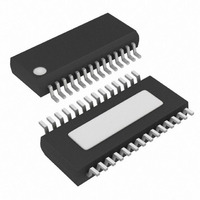
MAX1715EEI Maxim Integrated Products, MAX1715EEI Datasheet - Page 20

MAX1715EEI
Manufacturer Part Number
MAX1715EEI
Description
IC CTRLR DC DUAL STPDWN 28-QSOP
Manufacturer
Maxim Integrated Products
Type
Step-Down (Buck)r
Datasheet
1.MAX1715EEI.pdf
(25 pages)
Specifications of MAX1715EEI
Internal Switch(s)
No
Synchronous Rectifier
Yes
Number Of Outputs
2
Voltage - Output
1V, 1.8V, 2.5V, 3.3V, Adj
Current - Output
8A
Frequency - Switching
200kHz, 300kHz, 420kHz, 540kHz
Voltage - Input
2 ~ 28 V
Operating Temperature
-40°C ~ 85°C
Mounting Type
Surface Mount
Package / Case
28-QSOP
Power - Output
640mW
Output Voltage
1 V to 5.5 V, 3.3 V, 2.5 V
Output Current
8 A
Input Voltage
2 V to 28 V
Mounting Style
SMD/SMT
Maximum Operating Temperature
+ 85 C
Minimum Operating Temperature
- 40 C
Case
SSOP
Dc
05+
Lead Free Status / RoHS Status
Contains lead / RoHS non-compliant
Available stocks
Company
Part Number
Manufacturer
Quantity
Price
Part Number:
MAX1715EEI
Manufacturer:
MAXIM/美信
Quantity:
20 000
Company:
Part Number:
MAX1715EEI+
Manufacturer:
MAXIM
Quantity:
583
Part Number:
MAX1715EEI+
Manufacturer:
MAXIM/美信
Quantity:
20 000
Company:
Part Number:
MAX1715EEI+T
Manufacturer:
MAX
Quantity:
7 400
Part Number:
MAX1715EEI+T
Manufacturer:
MAXIM/美信
Quantity:
20 000
Part Number:
MAX1715EEI-T
Manufacturer:
MAXIM/美信
Quantity:
20 000
Company:
Part Number:
MAX1715EEI-TG069
Manufacturer:
MAXIN
Quantity:
2 268
Part Number:
MAX1715EEI-TG069
Manufacturer:
MAXOM
Quantity:
20 000
Ultra-High Efficiency, Dual Step-Down
Controller for Notebook Computers
20
power dissipation (PD) due to resistance occurs at
minimum battery voltage:
Generally, a small high-side MOSFET is desired in
order to reduce switching losses at high input voltages.
However, the R
power-dissipation limits often limits how small the MOS-
FET can be. Again, the optimum occurs when the
switching (AC) losses equal the conduction (R
losses. High-side switching losses don’t usually
become an issue until the input is greater than approxi-
mately 15V.
Switching losses in the high-side MOSFET can become
an insidious heat problem when maximum AC adapter
voltages are applied, due to the squared term in the
CV
you’ve chosen for adequate R
voltages becomes extraordinarily hot when subjected
to V
Calculating the power dissipation in Q1 due to switch-
ing losses is difficult since it must allow for difficult
quantifying factors that influence the turn-on and turn-
off times. These factors include the internal gate resis-
tance, gate charge, threshold voltage, source
inductance, and PC board layout characteristics. The
following switching loss calculation provides only a
very rough estimate and is no substitute for bread-
board evaluation, preferably including a verification
using a thermocouple mounted on Q1:
where C
and I
(1A typ).
For the low-side MOSFET, Q2, the worst-case power
dissipation always occurs at maximum battery voltage:
The absolute worst case for MOSFET power dissipation
occurs under heavy overloads that are greater than
I
the current limit and cause the fault latch to trip. To pro-
tect against this possibility, you must “overdesign” the
circuit to tolerate:
LOAD(MAX)
PD(Q1 resistance)
2
IN(MAX)
F switching loss equation. If the high-side MOSFET
______________________________________________________________________________________
I
GATE
LOAD
PD(Q1 switching)
PD(Q2)
RSS
, reconsider your choice of MOSFET.
is the peak gate-drive source/sink current
= I
but are not quite high enough to exceed
is the reverse transfer capacitance of Q1
LIMIT(HIGH)
DS(ON)
=
⎛
⎜
⎜
⎝
1 - V
V
IN MAX
=
(
=
⎛
⎜
⎜
⎝
required to stay within package
OUT
C
V
IN MIN
V
RSS
)
+ (LIR / 2)
OUT
(
⎞
⎟
⎟
⎠
I
LOAD
×
V
)
IN(MAX)
⎞
⎟
⎟
⎠
DS(ON)
I
I
LOAD
2
GATE
×
✕
R
2
I
2
LOAD(MAX)
DS ON
× ×
at low battery
×
f I
( )
R
LOAD
DS ON
( )
DS(ON)
)
where I
allowed by the current-limit circuit, including threshold
tolerance and on-resistance variation. This means that
the MOSFETs must be very well heatsinked. If short-cir-
cuit protection without overload protection is enough, a
normal I
ponent stresses.
Choose a Schottky diode (D1) having a forward voltage
low enough to prevent the Q2 MOSFET body diode
from turning on during the dead time. As a general
rule, a diode having a DC current rating equal to 1/3 of
the load current is sufficient. This diode is optional and
can be removed if efficiency isn’t critical.
The output voltage adjust range for continuous-con-
duction operation is restricted by the nonadjustable
500ns (max) minimum off-time one-shot. For best
dropout performance, use the slowest (200kHz) on-
time setting. When working with low input voltages, the
duty-factor limit must be calculated using worst-case
values for on- and off-times. Manufacturing tolerances
and internal propagation delays introduce an error to
the TON K-factor. This error is greater at higher fre-
quencies (Table 5). Also, keep in mind that transient
response performance of buck regulators operated
close to dropout is poor, and bulk output capacitance
must often be added (see the VSAG equation in the
Design Procedure).
Dropout design example: V
= 300kHz. The required duty is (V
V
case on-time is (V
✕
is:
which meets the required duty.
Remember to include inductor resistance and MOSFET
on-state voltage drops (V
dropout duty-factor calculations.
Ceramic capacitors have advantages and disadvan-
tages. They have ultra-low ESR and are noncom-
bustible, relatively small, and nonpolarized. They are
also expensive and brittle, and their ultra-low ESR char-
acteristic can result in excessively high ESR zero fre-
quencies (affecting stability). In addition, their relatively
low capacitance value can cause output overshoot
_________________Application Issues
SW
3.35µs-V
DUTY
) = (2V + 0.1V) / (3.0V - 0.1V) = 72.4%. The worst-
LIMIT(HIGH)
LOAD
=
t
ON(MIN)
✕
All-Ceramic-Capacitor Application
90% = 2.08µs. The IC duty-factor limitation
value can be used for calculating com-
t
ON(MIN)
OUT
+
t
OFF(MAX)
is the maximum valley current
+ 0.075) / V
SW
Dropout Performance
IN
) when doing worst-case
=
2.08 s 500ns
= 3V min, V
IN
OUT
2.08 s
μ
✕
+
μ
K = 2.075V / 3V
+ V
SW
OUT
=
) / (V
80.6%
= 2V, f
IN
-


