MAX1715EEI Maxim Integrated Products, MAX1715EEI Datasheet - Page 22
MAX1715EEI
Manufacturer Part Number
MAX1715EEI
Description
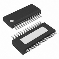
IC CTRLR DC DUAL STPDWN 28-QSOP
Manufacturer
Maxim Integrated Products
Type
Step-Down (Buck)r
Datasheet
1.MAX1715EEI.pdf
(25 pages)
Specifications of MAX1715EEI
Internal Switch(s)
No
Synchronous Rectifier
Yes
Number Of Outputs
2
Voltage - Output
1V, 1.8V, 2.5V, 3.3V, Adj
Current - Output
8A
Frequency - Switching
200kHz, 300kHz, 420kHz, 540kHz
Voltage - Input
2 ~ 28 V
Operating Temperature
-40°C ~ 85°C
Mounting Type
Surface Mount
Package / Case
28-QSOP
Power - Output
640mW
Output Voltage
1 V to 5.5 V, 3.3 V, 2.5 V
Output Current
8 A
Input Voltage
2 V to 28 V
Mounting Style
SMD/SMT
Maximum Operating Temperature
+ 85 C
Minimum Operating Temperature
- 40 C
Case
SSOP
Dc
05+
Lead Free Status / RoHS Status
Contains lead / RoHS non-compliant
Available stocks
Company
Part Number
Manufacturer
Quantity
Price

Part Number:
MAX1715EEI
Manufacturer:
MAXIM/美信
Quantity:
20 000
Company:
Part Number:
MAX1715EEI+
Manufacturer:
MAXIM
Quantity:
583
Part Number:
MAX1715EEI+
Manufacturer:
MAXIM/美信
Quantity:
20 000
Company:
Part Number:
MAX1715EEI+T
Manufacturer:
MAX
Quantity:
7 400
Part Number:
MAX1715EEI+T
Manufacturer:
MAXIM/美信
Quantity:
20 000
Part Number:
MAX1715EEI-T
Manufacturer:
MAXIM/美信
Quantity:
20 000
Company:
Part Number:
MAX1715EEI-TG069
Manufacturer:
MAXIN
Quantity:
2 268
Part Number:
MAX1715EEI-TG069
Manufacturer:
MAXOM
Quantity:
20 000


Ultra-High Efficiency, Dual Step-Down
Controller for Notebook Computers
value.
Careful PC board layout is critical to achieving low
switching losses and clean, stable operation. This is
especially true for dual converters, where one channel
can affect the other. The switching power stages require
particular attention (Figure 11). Refer to the MAX1715
EV kit data sheet for a specific layout example.
If possible, mount all of the power components on the
top side of the board with their ground terminals flush
against one another. Follow these guidelines for good
PC board layout:
• Isolate the power components on the top side from
• Use a star ground connection on the power plane to
22
Figure 10. 5V-Powered, 8A CPU Buck Regulator
switching frequency and a much smaller inductor
the sensitive analog components on the bottom side
with a ground shield. Use a separate PGND plane
under the OUT1 and OUT2 sides (called PGND1 and
PGND2). Avoid the introduction of AC currents into
the PGND1 and PGND2 ground planes. Run the
power plane ground currents on the top side only, if
possible.
minimize the crosstalk between OUT1 and OUT2.
______________________________________________________________________________________
PC Board Layout Guidelines
ON/OFF
100k
0.22μF
V
CC
1μF
ON2
REF
PGOOD
ILIM V
TON
CC
MAX1715
20Ω
V+
SKIP
PGND
AGND
OUT2
BST2
V
DH2
DL2
LX2
FB2
DD
• Keep the high-current paths short, especially at the
• Tie AGND and PGND together close to the IC. Do
• Keep the power traces and load connections short.
• LX_ and PGND connections to the synchronous rec-
• When trade-offs in trace lengths must be made, it’s
0.1μF
1μF
ground terminals. This practice is essential for sta-
ble, jitter-free operation.
not connect them together anywhere else. Carefully
follow the grounding instructions under Step 4 of the
Layout Procedure.
This practice is essential for high efficiency. Using
thick copper PC boards (2oz vs. 1oz) can enhance
full-load efficiency by 1% or more. Correctly routing
PC board traces is a difficult task that must be
approached in terms of fractions of centimeters,
where a single milliohm of excess trace resistance
causes a measurable efficiency penalty.
tifiers for current limiting must be made using Kelvin
sense connections to guarantee the current-limit
accuracy. With SO-8 MOSFETs, this is best done by
routing power to the MOSFETs from outside using
the top copper layer, while tying in PGND and LX_
inside (underneath) the SO-8 package.
preferable to allow the inductor charging path to be
4.5V TO 5.5V
V
IN
IRF7805
IRF7805
C1
4 x 10μF/25V
0.5μH
L1
C2
3 x 470μF
KEMET T510
2.5V AT 7A
V
OUT
Related parts for MAX1715EEI
Image
Part Number
Description
Manufacturer
Datasheet
Request
R

Part Number:
Description:
MAX7528KCWPMaxim Integrated Products [CMOS Dual 8-Bit Buffered Multiplying DACs]
Manufacturer:
Maxim Integrated Products
Datasheet:
Part Number:
Description:
Single +5V, fully integrated, 1.25Gbps laser diode driver.
Manufacturer:
Maxim Integrated Products
Datasheet:
Part Number:
Description:
Single +5V, fully integrated, 155Mbps laser diode driver.
Manufacturer:
Maxim Integrated Products
Datasheet:
Part Number:
Description:
VRD11/VRD10, K8 Rev F 2/3/4-Phase PWM Controllers with Integrated Dual MOSFET Drivers
Manufacturer:
Maxim Integrated Products
Datasheet:
Part Number:
Description:
Highly Integrated Level 2 SMBus Battery Chargers
Manufacturer:
Maxim Integrated Products
Datasheet:
Part Number:
Description:
Current Monitor and Accumulator with Integrated Sense Resistor; ; Temperature Range: -40°C to +85°C
Manufacturer:
Maxim Integrated Products
Part Number:
Description:
TSSOP 14/A�/RS-485 Transceivers with Integrated 100O/120O Termination Resis
Manufacturer:
Maxim Integrated Products
Part Number:
Description:
TSSOP 14/A�/RS-485 Transceivers with Integrated 100O/120O Termination Resis
Manufacturer:
Maxim Integrated Products
Part Number:
Description:
QFN 16/A�/AC-DC and DC-DC Peak-Current-Mode Converters with Integrated Step
Manufacturer:
Maxim Integrated Products
Part Number:
Description:
TDFN/A/65V, 1A, 600KHZ, SYNCHRONOUS STEP-DOWN REGULATOR WITH INTEGRATED SWI
Manufacturer:
Maxim Integrated Products
Part Number:
Description:
Integrated Temperature Controller f
Manufacturer:
Maxim Integrated Products
Part Number:
Description:
SOT23-6/I�/45MHz to 650MHz, Integrated IF VCOs with Differential Output
Manufacturer:
Maxim Integrated Products
Part Number:
Description:
SOT23-6/I�/45MHz to 650MHz, Integrated IF VCOs with Differential Output
Manufacturer:
Maxim Integrated Products
Part Number:
Description:
EVALUATION KIT/2.4GHZ TO 2.5GHZ 802.11G/B RF TRANSCEIVER WITH INTEGRATED PA
Manufacturer:
Maxim Integrated Products
Part Number:
Description:
QFN/E/DUAL PCIE/SATA HIGH SPEED SWITCH WITH INTEGRATED BIAS RESISTOR
Manufacturer:
Maxim Integrated Products
Datasheet: