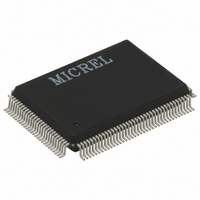
KSZ8993MI Micrel Inc, KSZ8993MI Datasheet - Page 40

KSZ8993MI
Manufacturer Part Number
KSZ8993MI
Description
IC SWITCH 10/100 W/TXRX 128PQFP
Manufacturer
Micrel Inc
Specifications of KSZ8993MI
Applications
*
Mounting Type
Surface Mount
Package / Case
128-MQFP, 128-PQFP
Number Of Primary Switch Ports
3
Internal Memory Buffer Size
32
Operating Supply Voltage (typ)
1.8/2.5/3.3V
Fiber Support
Yes
Integrated Led Drivers
Yes
Phy/transceiver Interface
MII/SNI
Power Supply Type
Analog/Digital
Package Type
PQFP
Data Rate (typ)
10/100Mbps
Vlan Support
Yes
Operating Temperature (max)
85C
Operating Temperature (min)
-40C
Pin Count
128
Mounting
Surface Mount
Jtag Support
No
Operating Supply Voltage (max)
1.89/3.465V
Operating Supply Voltage (min)
1.71/3.135V
Power Dissipation
800mW
Supply Current
0.1/0.19A
Operating Temperature Classification
Industrial
Data Rate
100Mbps
Lead Free Status / RoHS Status
Lead free / RoHS Compliant
Other names
576-2124
KSZ8993MI
KSZ8993MI
Available stocks
Company
Part Number
Manufacturer
Quantity
Price
Company:
Part Number:
KSZ8993MI
Manufacturer:
MICREL
Quantity:
1 900
Part Number:
KSZ8993MI
Manufacturer:
KENDIN
Quantity:
20 000
2. Enable I
3. Check to ensure that the KSZ8993M reset signal input, RST_N (pin 67), is properly connected to the external
4. Program the desired configuration data into the EEPROM.
5. Place the EEPROM on the board and power up the board.
6. Assert an active-low reset to the RST_N pin of the KSZ8993M. After reset is de-asserted, the KSZ8993M will
Note: For proper operation, check to ensure that the KSZ8993M PWRDN input signal (pin 36) is not asserted
during the reset operation. The PWRDN input is active low.
I
In managed mode, the KSZ8993M can be configured as an I
(external controller/CPU) has complete programming access to the KSZ8993M’s 128 registers. Programming
access includes the Global Registers, Port Registers, Advanced Control Registers and indirect access to the
“Static MAC Table”, “VLAN Table”, “Dynamic MAC Table,” and “MIB Counters.” The tables and counters are
indirectly accessed via registers 110 thru 120.
In I
registers is similar to addressing Atmel’s AT24C02 EEPROM’s memory locations. Details of I
operations and related timing information can be found in the AT24C02 Datasheet.
Two fixed 8 bits device addresses are used to address the KSZ8993M in I
other is for write. The addresses are as follow:
The following is a sample procedure for programming the KSZ8993M using the I
1. Enable I
2. Power up the board and assert reset to the KSZ8993M. After reset, the “Start Switch” bit (register 1 bit 0) will
3. Configure the desired register settings in the KSZ8993M, using the I
4. Read back and verify the register settings in the KSZ8993M, using the I
5. Write a ‘1’ to the “Start Switch” bit to start the KSZ8993M with the programmed settings.
Note: The “Start Switch” bit cannot be set to ‘0’ to stop the switch after an ‘1’ is written to this bit. Thus, it is
recommended that all switch configuration settings are programmed before the “Start Switch” bit is set to ‘1’.
Some of the configuration settings, such as “Aging enable”, “Auto Negotiation Enable”, “Force Speed” and “Power
down” can be programmed after the switch has been started.
SPI Slave Serial Bus Configuration
In managed mode, the KSZ8993M can be configured as a SPI slave device. In this mode, a SPI master device
(external controller/CPU) has complete programming access to the KSZ8993M’s 128 registers. Programming
access includes the Global Registers, Port Registers, Advanced Control Registers and indirect access to the
“Static MAC Table”, “VLAN Table”, “Dynamic MAC Table” and “MIB Counters”. The tables and counters are
indirectly accessed via registers 110 thru 120.
The KSZ8993M supports two standard SPI commands: ‘0000_0011’ for data read and ‘0000_0010’ for data write.
SPI multiple read and multiple write are also supported by the KSZ8993M to expedite register read back and
register configuration, respectively.
2
Micrel, Inc.
October 2008
C Slave Serial Bus Configuration
2
“00”.
reset source at the board level.
begin reading the configuration data from the EEPROM. The KSZ8993M will check that the first byte read
from the EEPROM is “93”. If this value is correct, EEPROM configuration will continue. If not, EEPROM
configuration access is denied and all other data sent from the EEPROM will be ignored by the KSZ8993M.
The configuration access time (t
“01”.
be set to ‘0’.
C slave mode, the KSZ8993M operates like other I
2
2
C master mode by setting the KSZ8993M strap-in pins, PS[1:0] (pins 100 and 101, respectively) to
C slave mode by setting the KSZ8993M strap-in pins PS[1:0] (pins 100 and 101, respectively) to
1011_1111 <read>
1011_1110 <write>
prgm
) is less than 15ms.
40
2
C slave devices. Addressing the KSZ8993M’s 8 bit
2
C slave device. In this mode, an I
2
C write operation.
2
C read operation.
2
C slave mode. One is for read; the
2
C slave serial bus:
2
C master device
M9999-020606
KSZ8993M/ML
2
C read/write


