EVAL-AD7689EDZ Analog Devices Inc, EVAL-AD7689EDZ Datasheet - Page 2
EVAL-AD7689EDZ
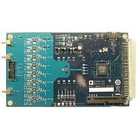
Manufacturer Part Number
EVAL-AD7689EDZ
Description
BOARD EVAL AD7689
Manufacturer
Analog Devices Inc
Series
PulSAR®r
Specifications of EVAL-AD7689EDZ
Number Of Adc's
1
Number Of Bits
16
Sampling Rate (per Second)
250k
Data Interface
Serial
Inputs Per Adc
8 Single Ended
Input Range
±VREF
Power (typ) @ Conditions
12.5mW @ 250kSPS, 5 V
Voltage Supply Source
Single Supply
Operating Temperature
-40°C ~ 85°C
Utilized Ic / Part
AD7689
Silicon Manufacturer
Analog Devices
Application Sub Type
ADC
Kit Application Type
Data Converter
Silicon Core Number
AD7689
Lead Free Status / RoHS Status
Lead free / RoHS Compliant


AD7682/AD7689
TABLE OF CONTENTS
Features .............................................................................................. 1
Applications ....................................................................................... 1
Functional Block Diagram .............................................................. 1
General Description ......................................................................... 1
Revision History ............................................................................... 2
Specifications ..................................................................................... 3
Absolute Maximum Ratings ............................................................ 8
Pin Configurations and Function Descriptions ........................... 9
Typical Performance Characteristics ........................................... 11
Terminology .................................................................................... 14
Theory of Operation ...................................................................... 15
REVISION HISTORY
6/09—Rev. A to Rev. B
Changes Table 6 ................................................................................ 8
Changes to Figure 37 ...................................................................... 25
Changes to Figure 38 ...................................................................... 26
3/09—Rev. 0 to Rev. A
Changes to Features Section, Applications Section, and
Figure 1 .............................................................................................. 1
Added Table 2; Renumbered Sequentially .................................... 3
Changed VREF to V
Changes to Table 3 ............................................................................ 5
Changes to Table 4 ............................................................................ 6
Changes to Table 5 ............................................................................ 7
Deleted Endnote 2 in Table 6 .......................................................... 8
Changes to Figure 4, Figure 5, and Table 7 ................................... 9
Changes to Figure 6, Figure 9, and Figure 10 ............................. 11
Changes to Figure 22 ...................................................................... 13
Changes to Overview Section and Converter Operation
Section .............................................................................................. 15
Changes to Table 8 .......................................................................... 16
Changes to Figure 26 and Figure 27 ............................................. 17
Changes to Bipolar Single Supply Section and Analog Inputs
Section .............................................................................................. 18
Changes to Internal Reference/Temperature Sensor Section ... 20
Timing Specifications .................................................................. 6
ESD Caution .................................................................................. 8
Overview ...................................................................................... 15
Converter Operation .................................................................. 15
Transfer Functions...................................................................... 16
Typical Connection Diagrams .................................................. 17
Analog Inputs .............................................................................. 18
Driver Amplifier Choice ............................................................ 20
REF
.................................................................... 4
Rev. B | Page 2 of 32
Digital Interface .............................................................................. 23
Application Hints ........................................................................... 30
Outline Dimensions ....................................................................... 31
Added Figure 31; Renumbered Sequentially .............................. 20
Changes to External Reference and Internal Buffer Section and
External Reference Section ........................................................... 21
Added Figure 32 and Figure 33 .................................................... 21
Changes to Power Supply Section ................................................ 22
Changes to Digital Interface Section, Reading/Writing After
Conversion, Any Speed Hosts Section, and Configuration
Register, CFG Section .................................................................... 23
Changes to Table 10 ....................................................................... 24
Added General Timing Without a Busy Indicator Section and
Figure 37 .......................................................................................... 25
Added General Timing With a Busy Indicator Section and
Figure 38 .......................................................................................... 26
Added Channel Sequencer Section and Figure 39 ..................... 27
Changes to Read/Write Spanning Conversion Without a Busy
Indicator Section and Figure 41 ................................................... 28
Changes to Read/Write Spanning Conversion with a Busy
Indicator and Figure 43 ................................................................. 29
Changes to Evaluating AD7682/AD7689 Performance
Section .............................................................................................. 30
Added Exposed Pad Notation to Outline Dimensions ............. 31
Changes to Ordering Guide .......................................................... 31
5/08—Revision 0: Initial Version
Voltage Reference Output/Input .............................................. 20
Power Supply ............................................................................... 22
Supplying the ADC from the Reference .................................. 22
Reading/Writing During Conversion, Fast Hosts .................. 23
Reading/Writing After Conversion, Any Speed Hosts .......... 23
Reading/Writing Spanning Conversion, Any Speed Host .... 23
Configuration Register, CFG .................................................... 23
General Timing Without a Busy Indicator ............................. 25
General Timing with a Busy Indicator .................................... 26
Channel Sequencer .................................................................... 27
Read/Write Spanning Conversion Without a Busy
Indicator ...................................................................................... 28
Read/Write Spanning Conversion with a Busy Indicator ..... 29
Layout .......................................................................................... 30
Evaluating AD7682/AD7689 Performance ............................ 30
Ordering Guide .......................................................................... 31
Related parts for EVAL-AD7689EDZ
Image
Part Number
Description
Manufacturer
Datasheet
Request
R


Part Number:
Description:
BOARD EVAL FOR SI270X-A
Manufacturer:
Silicon Laboratories Inc
Datasheet:

Part Number:
Description:
BUCK CONV REF DESIGN KIT IP1201
Manufacturer:
International Rectifier
Datasheet:
Part Number:
Description:
BOARD DEMO SYNC DUAL BUCK CNVTER
Manufacturer:
International Rectifier
Datasheet:
Part Number:
Description:
BOARD DEMO SYNC BUCK CONVETER
Manufacturer:
International Rectifier
Datasheet:

Part Number:
Description:
EVALBOARD/EB Omnidirectional microphone - Analog
Manufacturer:
Analog Devices
Datasheet:
Part Number:
Description:
EVALBOARD/EB Omnidirectional microphone - Analog
Manufacturer:
Analog Devices
Datasheet:


Part Number:
Description:
BOARD EVAL LED DRIVER LT3756
Manufacturer:
Linear Technology
Datasheet:

Part Number:
Description:
BOARD EVAL FOR AD7741/7742
Manufacturer:
Analog Devices Inc
Datasheet:

Part Number:
Description:
±1.7g Dual-Axis IMEMS Accelerometer Evaluation Board
Manufacturer:
Analog Devices Inc
Datasheet:

Part Number:
Description:
IC MULTIPLIER ANALOG 8-SOIC T/R
Manufacturer:
Analog Devices Inc
Datasheet:

Part Number:
Description:
IC ANALOG MULTIPLIER 8-DIP
Manufacturer:
Analog Devices Inc
Datasheet:
Part Number:
Description:
IC ANALOG MULTIPLIER 8-SOIC
Manufacturer:
Analog Devices Inc
Datasheet:
Part Number:
Description:
IC ANALOG MULTIPLIER 8-DIP
Manufacturer:
Analog Devices Inc
Datasheet: